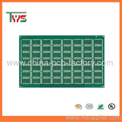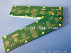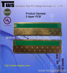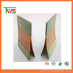

Gold Plated Controlled Impedance PCB
| Place of Origin: | Zhejiang |
|---|
Company Profile
| Location: | Shenzhen, Guangdong, China (Mainland) |
|---|---|
| Business Type: | Manufacturer |
| Main Products: | Multi Layer PCB, Double Sided PCB, Fr4 PCB Board |
Product Description
Gold Plated Controlled Impedance PCB Board 24 Layer Double Sided
Application
Products are applied to a wide range of High-tech industries such as: LED, telecommunication, computer application, lighting, game machine, industrial control, power, automobile and high-end consumer electronics, ect. By unremitting work and effort to the marketing, products exports to American, Canada, Europe counties, Africa and other Asia-pacific countries
Specifications
|
|
High precision prototype |
PCB bulk production |
|
|
Max Layers |
1-28 layers |
1-14 layers |
|
|
MIN Line width(mil) |
3mil |
4mil |
|
|
MIN Line space(mil) |
3mil |
4mil |
|
|
Min via (mechanical drilling) |
Board thickness≤1.2mm |
0.15mm |
0.2mm |
|
Board thickness≤2.5mm |
0.2mm |
0.3mm |
|
|
Board thickness2.5mm |
Aspect Ration≤13:1 |
Aspect Ration≤13:1 |
|
|
Aspect Ration |
Aspect Ration≤13:1 |
Aspect Ration≤13:1 |
|
|
Board thickness |
MAX |
8mm |
7mm |
|
MIN |
2 layers:0.2mm;4 layers:0.35mm;6 layers:0.55mm;8 layers:0.7mm;10 layers:0.9mm |
2 layers:0.2mm;4 layers:0.4mm;6 layers:0.6mm;8layers:0.8mm |
|
|
MAX Board size |
610*1200mm |
610*1200mm |
|
|
Max copper thickness |
0.5-6oz |
0.5-6oz |
|
|
Immersion Gold/ Gold Plated Thickness |
Immersion Gold:Au,1—8u” |
|
|
|
Hole copper thick |
25um 1mil |
25um 1mil |
|
|
Tolerance |
Board thickness |
Board thickness≤1.0mm:+/-0.1mm |
Board thickness≤1.0mm:+/-0.1mm |
|
Outline Tolerance |
≤100mm:+/-0.1mm |
≤100mm:+/-0.13mm | |


