
.gif)
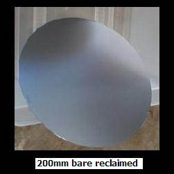
solar wafer
| Place of Origin: | Hebei |
|---|
Company Profile
| Location: | Shijiazhuang, Hebei, China (Mainland) |
|---|---|
| Business Type: | Manufacturer, Trading Company |
Product Detail
| Model No.: | 8' |
|---|---|
| Application: | Solar Thermal |
| Brand Name: | jinglong |
Product Description
Item | Spec | |
Crystal structure | Mono-crystalline | |
Crystal method | CZ | |
Conductance Type | P | |
Dopant | B | |
dimension | 125*125±0.4 | 125*125±0.4 |
Diameter | Φ150±0.4 | Φ165±0.4 |
Wafer thickness range | 190/200±20μm | 190/200±20μm |
Crystal orientation | <100>±1 | <100>±1 |
Resistivity( Ω.cm) | 1-3/3-6 | 1-3/3-6 |
Lifetime( μs) | ≥15 | ≥15 |
Carbon concentration( atoms/cm3 ) | ≤5*1016 | ≤5*1016 |
Oxygen concentration( atoms/cm3 ) | ≤0.95*1018 | ≤0.95*1018 |
Etching Pit( pcs/cm3 ) | ≤2000 | ≤2000 |
TTV | ≤30μm | ≤30μm |
Camber | ≤30μm | ≤30μm |
Saw mark | ≤15μm(depth) | ≤15μm(depth) |
Wafer surface | No crack, obvious pits, surface clean, no abnormal spots no pinholes. | |
Gap | No | |
Edge defect | Edge defect width≤0.2mm,extention≤0.5mm with total quantity≤2,,distance≥30mm | |
Luminance edge | Length≤1/2 of wafer dimension, width≤1/3 of wafer thickness | |
.jpg)
.jpg)
