
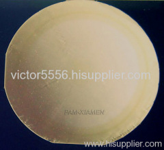
Semiconductor SiC Wafer or SiC(Silicon Carbide)Wafer
| Payment Terms: | T/T |
|---|---|
| Place of Origin: | Fujian |
Company Profile
| Location: | Xiamen, Fujian, China (Mainland) |
|---|---|
| Business Type: | Manufacturer |
Product Description
PWAM offers semiconductor materials,SiC substate for GaN epitaxy device,power devices, high-temperature device and optoelectron
PWAM offers semiconductor materials,SiC substate(Epi-Ready) for GaN epitaxy device,power devices, high-temperature device and optoelectronic Devices.
PWAM offers semiconductor materials,SiC substate for GaN epitaxy device,power devices, high-temperature device and optoelectronic Devices.
PWAM offers SiC substate,N type and Semi-insulating. Available size:4Inch(100mm),3Inch(76.2mm),2Inch(50.80mm),30*30mm,20*20mm,10*10mm,5*5mm. polytype 4H and 6H in different quality grades,Micropipe Density (MPD): Free,<5/cm2,<10/cm2,<30/cm2,<50/cm2,<100/cm2.Application: for GaN epitaxy device,power devices, high-temperature device and optoelectronic Devices
Avalaible Plane:a-plane or c-plane 6H-SiC wafers and 4H-SiC wafers