
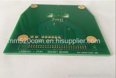
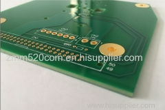
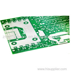
Multilayer PCB Circuit Boards Manufactur in Shenzhen
| Min. Order: | 1 Square Meter |
|---|---|
| Trade Term: | FOB,CIF,DAT,DAP,CPT,FCA,EXW |
| Payment Terms: | Paypal, L/C, D/P, D/A, T/T, WU, Money Gram |
| Supply Ability: | 1500squire meter/week |
| Place of Origin: | Guangdong |
Company Profile
| Location: | Shenzhen, Guangdong, China (Mainland) |
|---|---|
| Business Type: | Manufacturer |
Product Detail
| Model No.: | customized |
|---|---|
| Means of Transport: | Ocean, Air, Land |
| Number of Layers: | 4-Layer |
| Brand Name: | Hitech |
| Base Material: | FR4 High TG |
| Copper Thickness: | 1OZ |
| Board Thickness: | 1.2MM |
| Min. Hole Size: | 0.26MM |
| Min. Line Width: | 0.12MM |
| Min. Line Spacing: | 0.14 |
| Solder mask: | Green,Black,Blue,Red |
| Wrap and twist: | 5% |
| Profiling punching: | Routing, V-CUT, Beveling |
| Testing: | 100% E-Test |
| Standards: | IPC-A-610 E Class II-III |
| Mounting Production: | 6 SMT Lines |
| Through Hole Production: | 2 DIP Lines |
| Enclosure Assembly: | 2 Assembly Lines |
| Package: | Vacuum Skin Double-Sided |
| profiling punching: | Routing, V-CUT, Beveling |
| Production Capacity: | 1500squire meter/week |
| Packing: | 35*26*12mm/carton |
| Delivery Date: | 5-8 WDs |
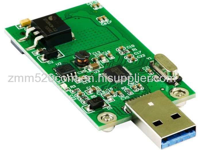
Product Description
Multilayer PCB Circuit Boards Manufactur in Shenzhen

1>Our Superiority is the Professionalism of our team.
- PCB And PCB Assembly For One-stop Service with Original Components According the BOM.
IC Imported from Digikey / Farnell etc.
- Low Cost with High Quality, Commitment of Quality Assurance.
- For 10 years Experience in PCB Field. ( Our Factory owns advanced
production equipment and experienced technical personnel. )
2> Detailed specification of manufaturing capacity:
NO | Item | Craft Capacity |
1 | Layer | 1-30 Layers |
2 | Base Material for PCB | FR4, CEM-1, TACONIC, Aluminium, High Tg Material, High Frequence ROGERS ,TEFLON, ARLON, Halogen-free Material |
3 | Rang of finish baords Thickness | 0.21-7.0mm |
4 | Max size of finish board | 900MM*900MM |
5 | Minimum Linewidth | 3mil (0.075mm) |
6 | Minimum Line space | 3mil (0.075mm) |
7 | Min space between pad to pad | 3mil (0.075mm) |
8 | Minimum hole diameter | 0.10 mm |
9 | Min bonding pad diameter | 10mil |
10 | Max proportion of drilling hole and board thickness | 1:12.5 |
11 | Minimum linewidth of Idents | 4mil |
12 | Min Height of Idents | 25mil |
13 | Finishing Treatment | HASL (Tin-Lead Free), ENIG(Immersion Gold), Immersion Silver , Gold Plating (Flash Gold), OSP, etc. |
14 | Soldermask | Green, White, Red, Yellow, Black, Blue, transparent photosensitive soldermask, Strippable soldermask. |
15 | Minimun thickness of soldermask | 10um |
16 | Color of silk-screen | White, Black, Yellow ect. |
17 | E-Testing | 100% E-Testing (High Voltage Testing); Flying Probe Testing |
18 | Other test | ImpedanceTesting,Resistance Testing, Microsection etc., |
19 | Date file format | GERBER FILE and DRILLING FILE, PROTEL SERIES, PADS2000 SERIES, Powerpcb SERIES, ODB++ |
20 | Special technological requirement | Blind & Buried Vias and High Thickness copper |
21 | Thickness of Copper | 0.5-14oz (18-490um) |
3> Quote Requirements for PCB and PCB Assembly project:
- Gerber File and Bom List;
- Quote Quantity;
- Advise your technical requirements for quoting reference;
- Clearly picturers of PCB or PCB Assembly Sample to us for reference;
- Test Mothod for PCB Assembly.
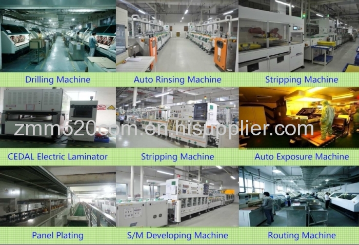
4> Equipment List
NO. | Machine Name | QTY | NO. | Machine Name | QTY |
1 | PRESS | 2 | 10 | Exposurer | 5 |
2 | X-Ray | 1 | 11 | Deveoloper | 3 |
3 | Brown-Oxidation | 1 | 12 | Auto V-cut | 1 |
4 | Drilling | 13 | 13 | AOI | 2 |
5 | Cutter | 1 | 14 | Routing | 7 |
6 | PTH | 1 | 15 | ETS | 12 |
7 | PAL | 1 | 16 | Fly Probe | 4 |
8 | PAT | 1 | 17 | YAMAHA SMT | 3 |
9 | Flash Gold | 1 | 18 | FUJI SMT | 4 |
5> PCB and PCB Assembly Lead time:
Description | Double side | Four Layers | Six Layers | Above Eight | HDI |
Sample | 4 | 7 | 9 | 9 | 12 |
Mass production | 7-9 | 10-12 | 13-15 | 16 | 20 |
Assembly | 7-9 | 15 | 16 | 18 | 25 |
6> T-SOAR can be trusted PCB Partner, We are waiting for cooperation with you anytime.
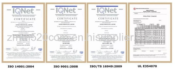
- UL, RoHS, ISO, SGS Certification Compliance.
- OEM Assembly, Design, Prototype Service.
- We will be responsible for the quality of our products,
- Survive by quality, Win by Price.
RFQ
Q1:What service do you have?
IBE: We provide turnkey solution including RD, PCB fabrication, SMT, plastic injection & metal, final assembly,testing and other value-added service.
Q2:What are the main products of your PCB/PCBA services?
IBE: Our PCB/PCBA services are mainly for the industries including Medical, Automotive, Energy, Metering/Measurements, Consumer Electronics.
Q3:Is IBE a factory or trade company?
IBE: IBE is a factory with PCB factory located in China and SMT assembly factories in both China & USA.
Q4:Can we inspect quality during production?
IBE: Yes, we are open and transparent on each production process with nothing to hide. We welcome customer inspect our production process and check in house.
Q5:How can we ensure our information should not let third party to see our design?
IBE: We are willing to sign NDA effect by customer side local law and promising to keep customers data in high confidential level.
Q6:What files required to get quotation from you?
IBE: For PCB quotation, please provide the Gerber data/files and indication of related technical requirements as well as any special requirement if you have.
For PCBA quotation, please provide Gerber data/ files and also BOM (bill of materials), and if you need us to do function test, please also provide the test instruction/procedure.
Q7:What is standard delivery term?
IBE: Delivery terms of EXW, FCA, FOB, DDU etc. are all available based on each quote.
Q8:How long does it take for PCB quote?
IBE: Normally 24 hours to 48 hours as soon as receive internal engineer evaluate confirmation.
Q9:Do you have any minimum order quantity (MOQ) requirement?
IBE: No, we do not have MOQ requirement, we can support your projects starting from prototypes to mass productions.
Email: sales10(at)hitechcircuits(dot)com