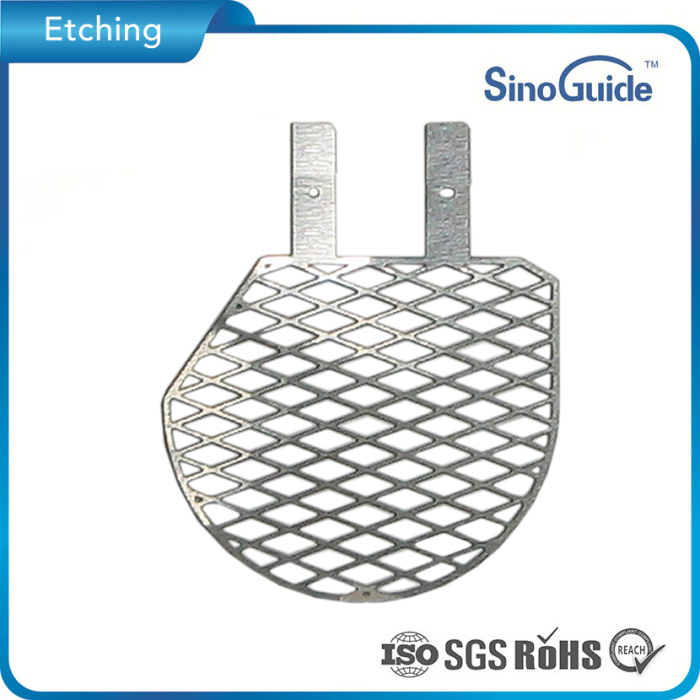
Photo Chemical Etching Nickel Anode Screen for Implantable Batteries
| Min. Order: | 100 Piece/Pieces |
|---|---|
| Trade Term: | EXW |
| Payment Terms: | T/T, WU, Money Gram |
| Supply Ability: | 30000 pcs/day |
| Place of Origin: | Guangdong |
Company Profile
| Location: | Shenzhen, Guangdong, China (Mainland) |
|---|---|
| Business Type: | Manufacturer, Trading Company |
Product Detail
| Model No.: | SinoguideScreen |
|---|---|
| Means of Transport: | Ocean, Air, Land |
| Brand Name: | Etched Screen |
| Name: | Nickel Anode Screen |
| Thickness: | 0.03mm-1.5mm |
| Tolerance: | +/-0.01mm |
| Size:: | 1*1mm2 - 300*500mm2 |
| Smallest Open Hole: | Smallest Open Hole |
| 0.1mm: | +/-0.025mm |
| Edge: | Burr free |
| Artwork:: | Ai/Coreldraw/PDF etc |
| MOQ:: | 500PCS |
| Supply Ability: | 100000pcs/day |
| Production Capacity: | 30000 pcs/day |
| Packing: | SinoGuide Packing or Customized |
| Delivery Date: | 3~5 working days |
Product Description
Photo Chemical Etching Nickel Anode Screen for Implantable Batteries
Applications:
Sinoguide's product capabilities include manufacturing RF, Microwave, Transistor, Hybrid component carriers, plates, flanges, bases, frames, lead frames, and other RF microwave devices to customers' specifications. Below is a sampling of some of the parts built to specifications for the RF and Microwave industries. Thin metal parts are made out of various metals and alloys (copper, brass, stainless steel, kovar) and are even manufactured out of other composite materials (FR4, Teflon, Duroid), along with different platings (typically nickel and/or gold plating). Below are pictures of gold plated carriers, plates, flanges, bases, frames, covers, lids, and other various types of small metal parts used in the RF, microwave, transistors and bi-polar transistor packages, and small housings.
Product Description | |
Product name: | Photo Chemical Etching Nickel Anode Screen for Implantable Batteries |
Material: | Stainless steel, copper, silicon steel plate,or customize |
Size: | According to customers |
Thickness: | 0.03-1.5mm is available |
Technique: | High precision etching |
Hole: | 0.01mm(customize) |
Spacing | 0.018mm(customize) |
Hole shape: | Round/ Square |
Surface finish: | Clean .no burr |
Features: | No burrs,No broken point,no plugging holes |
Application: | Fiber filter,Textile machines or customize |
Certificate: | RoHS,ISO |
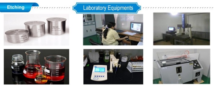
Inspection: | Two-dimension inspection machine,magnifier |
Other Related Items | |
Price: | According to product specification |
Sample Offer: | Within 3-6 days |
Payment: | T/T,L/C,Paypal,Western Union |
Lead time for mass production: | Within 6-10 days after payment |
Production ability: | 10000pcs/week |
Metal process methods available: | Stamping,Chemical etching,Laser cutting |
Acceptable file format: | DWG,DXF,IGES,PDF,JEPG |
Standard met: | Customer specification,2D CAD drawing |
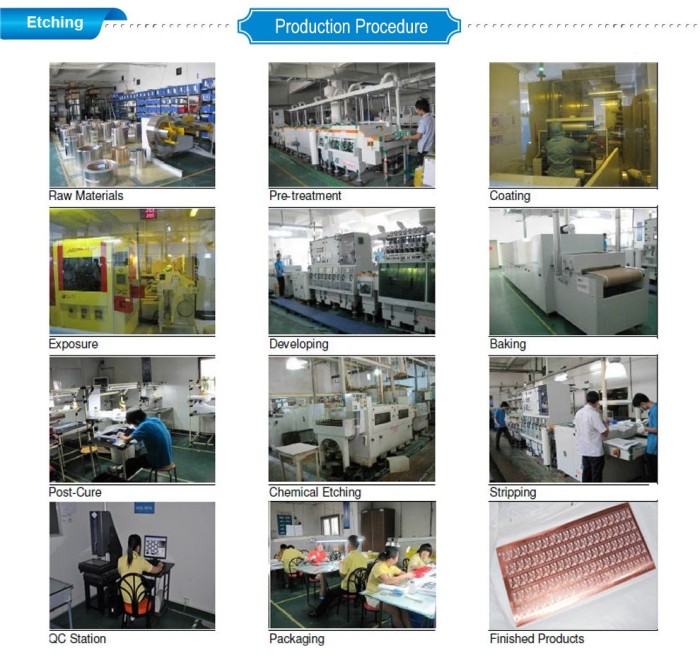
Advantages of Photo Etching:
•Low tooling cost, no need for expensive DIE/Mould
•Can fabricate more thinner metals(T=0.02-1.2 mm)
•No alteration process, the characteristics can be obtained as the designer intended
•High accuracy
•Various apertures, shapes and bar combinations
•Burr & Stress free manufacturing method
•Prototypes – fast turnaround to meet your needs
•High volume capabilities
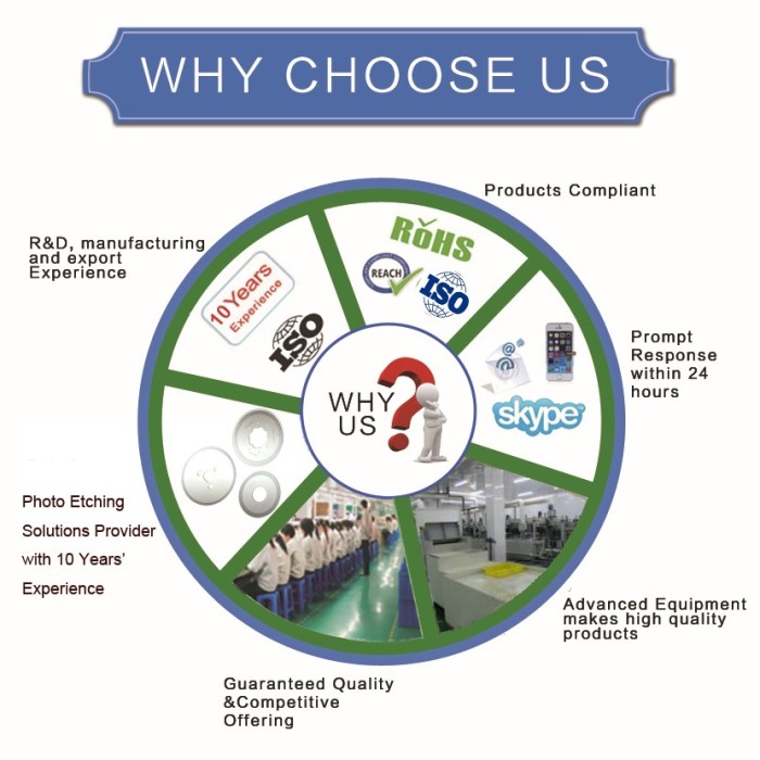
SinoGuide provides high quality and performance photo etching components for customers, further more, our high production capacity can also fulfill your high-volume orders and shorten the lead time.
SinoGuide is also a one-stop solution provider, we can also provide you value added service such plating, polishing, stamping, PVD coating etc.