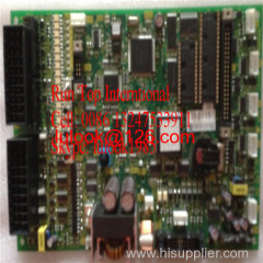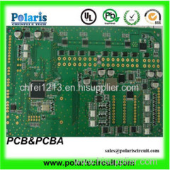
Power Amplifier PCB Board in China
| Place of Origin: | Hebei |
|---|
Company Profile
| Location: | Shijiazhuang, Hebei, China (Mainland) |
|---|---|
| Business Type: | Manufacturer |
Product Description
Layer count | 1-36 layers |
Min line width/space | 3mil/3mil |
Mim Mechanical drilling hole size | Board thickness≤1.2mm 0.15mm |
Board thickness≤2.5mm 0.2mm | |
Board thickness>1.2mm Aspect ratio≤15:1 | |
Finished board thickness | Max: 10mm |
Min: 2 layers-0.2mm; 4 layers-0.35mm; 6 layers-0.55mm; | |
8layers-0.7mm, 10layers-0.9mm | |
Finished copper thiciness | Inner layer/outer layer:6oz/10oz |
Max panel size | 610*1200mm |
Impedeance Tolerance | ±10% |
Min Dielectric thickness | 2mil |
Type of dielectric meterial | FR4,high TG,Flex,rigid,rigid-terial,High frequency material,PTFE material,heavy copperfoil,paperphenolic plate,BT,PI,Composite material,PTFE+ metal based |
Major Material supplier | FR4:Shengyi,ITEQ,Isola,KB,Arlon PTFE:Rogers,Taconic,Nelco,Wangling, Metal based meterial:Bergquist,Laird,Totking,ITEQ,Arlon,
|
Soldermask colour | green,red,blue,white,black,yellow |
Surface treatment | HASL ,immsersion gold,immersion silver,OSP,gold finger
|
Special process | Multilayer PCB with blind or buried vias, impedance control |
Quality control | AOI,100% electronic test |
Mount range | 0201,0402,0603.0805,1206,1210.chips,QFN,QFP,BGA,LGA,DSP,CSP assembly;through hole parts assembly |
Mount Accuracy | ±0.05MM |
Max PCB size | Sample:400*800mm;Volume 350*550mm |
Max components height | 25.4mm |
Min pitch for QPF/SOP/SOJ/IC | 0.3mm |
Min pitch for GSP/BGA | 0.3mm |
Test | AOI,eyes testing,function test,temperature cycling |


