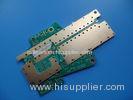
RF Amplifer Four Layer Hybrid PCB RO4003C Core And RO4450B Prepreg Combined
PCB parameters
| PCB SIZE | 93.5 x 68.92mm=1PCS |
| BOARD TYPE | |
| Number of Layers | Multilayer PCB, 4 layer PCB |
| Surface Mount Components | YES |
| Through Hole Components | NO |
| LAYER STACKUP | copper ------- 35um(1oz)+plate TOP layer |
| RO4003C 0.305mm (12mil) |
| copper ------- 35um(1oz) MidLayer 1 |
| RO4450B 0.101mm |
| copper ------- 35um(1oz) MidLayer 2 |
| FR-4 0.25mm |
| copper ------- 17um(0.5oz)+plate BOT Layer |
| TECHNOLOGY | |
| Minimum Trace and Space: | 5mil/6mil |
| Minmum / Maximum Holes: | 0.3/5.5mm |
| Number of Different Holes: | 7 |
| Number of Drill Holes: | 491 |
| Number of Milled Slots: | 0 |
| Number of Internal Cutouts: | 2 |
| Impedance Control: | no |
| Number of Gold finger: | 0 |
| BOARD MATERIAL | |
| Glass Epoxy: | RO4003C 0.305mm (12mil) and FR-4 0.25mm combined |
| Final foil external: | 1oz |
| Final foil internal: | 1oz |
| Final height of PCB: | 1.0mm ±0.1 |
| PLATING AND COATING | |
| Surface Finish | Immersion Gold (80.4%) 2 micoinch over 100 microinch nickel |
| Solder Mask Apply To: | TOP and Bottom, 12micron Minimum |
| Solder Mask Color: | Green, PSR-2000 GT600D, Taiyo Supplied. |
| Solder Mask Type: | LPSM |
| CONTOUR/CUTTING | Routing |
| MARKING | |
| Side of Component Legend | TOP. |
| Colour of Component Legend | White, IJR-4000 MW300, Taiyo Supplied. |
| Manufacturer Name or Logo: | Marked on the board in a conductor and leged FREE AREA |
| VIA | Plated through hole(PTH), via open |
| FLAMIBILITY RATING | UL 94-V0 Approval MIN. |
| DIMENSION TOLERANCE | |
| Outline dimension: | 0.0059" (0.15mm) |
| Board plating: | 0.0030" (0.076mm) |
| Drill tolerance: | 0.002" (0.05mm) |
| TEST | 100% Electrical Test prior shipment |
| APPLICATION: | RF Amplifier
|
| TYPE OF ARTWORK TO BE SUPPLIED | email file, Gerber RS-274-X, PCBDOC etc |
| SERVICE AREA | Worldwide, Globally. |
Advantages
a) RO4003C has stable dielectric constant over a broad frequency range. This makes it an ideal substrate for broadband applications.
b) Immersion gold PCB. Long storage time ( It can be stored for more than 1 year in vacuum bag)
c) No MOQ, low cost for small quantity prototypes and samples.
d) ISO certified PCB manufacturing factory.
e) Meeting your printed circuit board needs from PCB prototyping to mass volume production.
More Applications in Electronics
Wifi Module
Antena Wireless
Antena Wifi Usb
RF Transmitter
Frequency Converter
RF Module
PCB knowledge: Layer Stackup
The purpose of stackup is to interleave the thin laminates and the prepreg sheets in correct sequence and ensure correct layer-to-layer registration. The stackup of multilayer boards can be done in many different ways.
Among multilayer PCB's, 12- layer is the largest number of layers that can be produced easily in 1.6mm thick.
Hybrid PCB stack up
4 layer PCB, RO4350B combined with FR-4 Core.

Genuine RO4350B 4 layer PCB vs FR-4 4 layer PCB
Build-up of FR-4 PCB (4 layer) Build-up of RO4350B PCB (4 layer)
Copper track --- Layer 1 Copper track --- Layer 1
Prepreg(PP) RO4350B Core
Copper track --- Layer 2 Copper track --- Layer 2
FR-4 Core Rogers Prepreg(PP)
Copper track --- Layer 3 Copper track --- Layer 3
Prepreg(PP) RO4350B Core
Copper track --- Layer 4 Copper track --- Layer 4
 microsection, 12 layer PCB. FR-4
FAQ
How do you pack the PCBs?
PCBs are packed with Polyethylene air cushion film(vacuum plastic bags) per 20-25 pieces. Pearl cotton (Polyethylene foamed sheet) are put inside carton box.
The hardness


 microsection, 12 layer PCB. FR-4
