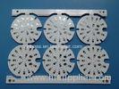

MCPCB 6061 Aluminum SilkscreenPCB HASL Lead Free For Led Panel Light
| Place of Origin: | Zhejiang |
|---|
Company Profile
| Location: | Shenzhen, Guangdong, China (Mainland) |
|---|---|
| Business Type: | Manufacturer |
Product Detail
| Model No.: | BIC-090231-A2 |
|---|
Product Description
MCPCB 6061 Aluminum Silkscreen PCB HASL Lead Free For Led Panel Light
PCB parameters
| PCB SIZE | 160 x 70mm=6PCS |
| BOARD TYPE | |
| Number of Layers | Single sided PCB |
| Surface Mount Components | YES |
| Through Hole Components | NO |
| LAYER STACKUP | copper ------- 35um(1oz) |
| 1W/MK dielectric material 75um | |
| Aluminum 6061 1.6mm | |
| TECHNOLOGY | |
| Minimum Trace and Space: | 16mil/25mil |
| Minmum / Maximum Holes: | 0 |
| Number of Different Holes: | 0 |
| Number of Drill Holes: | 0 |
| Number of Milled Slots: | 3 |
| Number of Internal Cutouts: | 0 |
| Impedance Control | no |
| BOARD MATERIAL | |
| Aluminum core: | 1W / MK dielectric material 75um |
| Thermal resistance(°C/W) | ≤0.45 |
| Breakdown Voltage(VDC) | 4000 |
| Final foil external: | 1oz |
| Final foil internal: | 0oz |
| Final height of PCB: | 1.6mm ±0.16 |
| PLATING AND COATING | |
| Surface Finish | Hot air soldering leveling(HASL),lead free, Sn>=2.54µm |
| Solder Mask Apply To: | TOP, 12micron Minimum |
| Solder Mask Color: | White, Taiyo PSR400 WT02 |
| Solder Mask Type: | LPSM |
| CONTOUR/CUTTING | Routing |
| MARKING | |
| Side of Component Legend | TOP |
| Colour of Component Legend | Black |
| Manufacturer Name or Logo: | Marked on the board in a conductor and leged FREE AREA |
| VIA | Non Plated Throught Hole (NPTH) |
| FLAMIBILITY RATING | UL 94-V0 Approval MIN. |
| DIMENSION TOLERANCE | |
| Outline dimension: | 0.0059" |
| Board plating: | 0.0029" |
| Drill tolerance: | 0.002" |
| TEST | 100% Electrical Test prior shipment |
| APPLICATION: | Led panel light |
| TYPE OF ARTWORK TO BE SUPPLIED | email file, Gerber RS-274-X, PCBDOC etc |
| SERVICE AREA | Worldwide, Globally. |
Advantages
a) Metal core PCB. Replace the fragile ceramic substrate, to obtain a better mechanical durability.
b) Optimization combination of power circuit and control circuit.
c) HASL surface finish. Excellent wetting during component soldering and it can avoid copper corrosion.
d) Meeting your printed circuit board needs from PCB prototyping to mass volume production.
e) ISO certified PCB manufacturing factory.
More Applications in Electronics
Frequency Inverter
5V Dc Power Supply
LTE Power Supply
Pyramid Power Supply
Server Power Supply

PCB knowledge: Frequently used Unit Conversion in PCB industry
1 inch= 25.4mm
1 inch= 1000mil
1 foot = 12 inch=0.3048 meter
1mm = 39.37mil
1mm = 1000µm
1µm = 39.37 micro inch
1oz = 35µm = 1.4mil = 305g/m²
1inch² = 0.0645dm² = 6.4516cm² = 645.16mm²
1ft² = 144 inch² = 0.09290304m² = 9.29dm²
1m² = 1549.9969 inch²
Multilayer PCB Stackup: 6 layer 0.062inch Finished Thickness
This is reference layer stackup. The stackup of multilayer PCB’s can be reached in many different ways.

FAQ
What's your minimum isolation of layers?
The minimum thickness of prepreg in inner layer is 0.06mm for prototypes, and thicker at 0.1mm for mass production.

