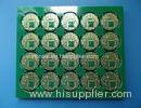

FR4 ER5.4 Blind Via PCB 4 Layer Immersion Gold For Bluetooth Receiver
| Place of Origin: | Zhejiang |
|---|
Company Profile
| Location: | Shenzhen, Guangdong, China (Mainland) |
|---|---|
| Business Type: | Manufacturer |
Product Detail
| Model No.: | BIC-089472-3C |
|---|
Product Description
FR4 ER5.4 Blind Via PCB 4 Layer Immersion Gold For Bluetooth Receiver
PCB parameters
| PCB SIZE | 150 x 160mm=20PCS |
| BOARD TYPE | |
| Number of Layers | Multilayer, 4 layer PCB |
| Surface Mount Components | YES |
| Through Hole Components | NO |
| LAYER STACKUP | copper ------- 17um(0.5oz)+plate TOP layer |
| Prepreg 1x2133 + 1x1080 + 1x2116 0.29mm | |
| copper ------- 17um(0.5oz) MidLayer 1 | |
| FR-4 0.89mm | |
| copper ------- 17um(0.5oz) MidLayer 2 | |
| Prepreg 1x2133 + 1x1080 + 1x2116 0.29mm | |
| copper ------- 17um(0.5oz)+plate BOT Layer | |
| TECHNOLOGY | |
| Minimum Trace and Space: | 3.9mil/6.1mil |
| Minmum / Maximum Holes: | 0.3/0.72mm |
| Number of Different Holes: | 10 |
| Number of Drill Holes: | 851 |
| Number of Milled Slots: | 36 |
| Number of Internal Cutouts: | 0 |
| Impedance Control | no |
| BOARD MATERIAL | |
| Glass Epoxy: | ITEQ IT140 TG>135, er<5.4 |
| Final foil external: | 1oz |
| Final foil internal: | 1oz |
| Final height of PCB: | 1.6mm ±0.16 |
| PLATING AND COATING | |
| Surface Finish | Immersion gold 0.025µm over 3µm Nickel |
| Solder Mask Apply To: | TOP and Bottom, 12micron Minimum |
| Solder Mask Color: | Gloss Green, Taiyo PSR-2000GT600D |
| Solder Mask Type: | LPSM |
| CONTOUR/CUTTING | Routing |
| MARKING | |
| Side of Component Legend | TOP |
| Colour of Component Legend | White |
| Manufacturer Name or Logo: | Marked on the board in a conductor and leged FREE AREA |
| VIA | Plated through hole(PTH), Blind via L1-L2 |
| FLAMIBILITY RATING | UL 94-V0 Approval MIN. |
| DIMENSION TOLERANCE | |
| Outline dimension: | 0.0059" |
| Board plating: | 0.0029" |
| Drill tolerance: | 0.002" |
| TEST | 100% Electrical Test prior shipment |
| APPLICATION: | Bluetooth receiver |
| TYPE OF ARTWORK TO BE SUPPLIED | email file, Gerber RS-274-X, PCBDOC etc |
| SERVICE AREA | Worldwide, Globally. |
Advantages
a) FR-4 UL94V0 material. RoHS compliant and suitable for thermal reliability needs,and Lead free assemblies with a maximum reflow temperature of 260.
b) Immersion gold PCB. High solderability, no stressing of circuit boards and less contamination of PCB surface.
c) 100% tests inclusive of electrical test and AOI inspection.High voltage test, Impedance control test, micro-section, solder-ability test, thermal stress test, reliability test, insulation resistance test and ionic contamination test etc.
d) ISO certified PCB manufacturing factory.
e) Delivery on time. We keep higher than 95% on-time-delivery rate.
More Applications in Electronics
Wireless Hub
Wifi 3G
Wifi Booster Antenna
USB Wlan Adapter
AC To DC Adapter
Design for Manufacture (1)
| Serial NO. | Procedure | Item | Manufacturing capability | ||
| Large volume (S<100 m²) | Middle volume (S<10 m²) | Prototype(S<1m²) | |||
| 1 | Inner layer (18um, 35um, 70um etc are finished copper. If not mentioned copper, finished 1oz is the default value ) | Min.isolation of layers | 0.1mm | 0.1mm | 0.06mm |
| 2 | Min.track and spacing | 5/5mil(18um) | 4/4mil(18um) | 3/3.5mil(18um) | |
| 3 | 5/5mil(35um) | 4/4mil(35um) | 3/4mil(35um) | ||
| 4 | 7/9mil(70um) | 6/8mil(70um) | 6/7mil(70um) | ||
| 5 | 9/11mil(105um) | 8/10mil(105um) | 8/9mil(105um) | ||
| 6 | 13/13mil(140um) | 12/12mil(140um) | 12/11mil(140um) | ||
| 7 | Min.distance from drill to conductor | 4 Layer 10mil,6 layer 10mil,8-12 layer 12mil | 4 layer 8mil,6 layer 8mil,8-12 layer 10mil,14-20 layer 14mil,22-32 layer 18mil | 4 layer 6mil,6 layer 6mil,8-14 layer 8mil,16-22 layer 12mil,24-32 layer 14mil | |
| 8 | Min.width of annular ring on inner layer | 4 Layer 10mil(35um),≥6 Layer 14mil(35um) | 4 Layer 8mil(35um),≥6 layer 12mil(35um) | 4 Layer 6mil(35um),≥6 Layer 10mil(35um) | |
|
| |||||

