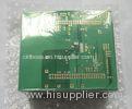

GPS FR4 6 Layer Pad PCB Via Plating CTI 175V-249V Quick Turn Circuit Boards
| Place of Origin: | Zhejiang |
|---|
Company Profile
| Location: | Shenzhen, Guangdong, China (Mainland) |
|---|---|
| Business Type: | Manufacturer |
Product Detail
| Model No.: | C5DS_0200_V01 |
|---|
Product Description
GPS FR4 6 Layer Pad PCB Via Plating CTI 175V-249V Quick Turn Circuit Boards
PCB Properties
| PCB SIZE | 93.25 x 104.12mm=1PCS |
| BOARD TYPE | |
| Number of Layers | Multilayer PCB, 6 Layer PCB |
| Surface Mount Components | YES |
| Through Hole Components | YES |
| LAYER STACKUP | copper ------- 18um(0.5oz)+plate TOP layer |
| Prepreg 7628 0.195mm | |
| copper ------- 18um(0.5oz) MidLayer 1 | |
| FR-4 0.1mm | |
| copper ------- 18um(0.5oz) MidLayer 2 | |
| Prepreg 7628 0.195mm | |
| copper ------- 18um(0.5oz) MidLayer 3 | |
| FR-4 0.1mm | |
| copper ------- 18um(0.5oz) MidLayer 4 | |
| Prepreg 7628 0.195mm | |
| copper ------- 18um(0.5oz)+plate BOT Layer | |
| TECHNOLOGY | |
| Minimum Trace and Space: | 4mil/4mil |
| Minmum / Maximum Holes: | 0.2/1.3mm |
| Number of Different Holes: | 11 |
| Number of Drill Holes: | 9840 |
| Number of Milled Slots: | 0 |
| Number of Internal Cutouts: | 0 |
| Impedance Control | no |
| BOARD MATERIAL | |
| Glass Epoxy: | FR-4 S1140, Tg 135. |
| Final foil external: | 1oz |
| Final foil internal: | 0.5oz |
| Final height of PCB: | 1.1mm ±0.1 |
| PLATING AND COATING | |
| Surface Finish | Immersion Gold (19.1%) 2µ" over 100µ" nickle |
| Solder Mask Apply To: | Top and Bottom, 12micon Minimum. |
| Solder Mask Color: | Green, LP-4G G-05, Nanya supplied |
| Solder Mask Type: | LPSM |
| CONTOUR/CUTTING | Routing |
| MARKING | |
| Side of Component Legend | TOP |
| Colour of Component Legend | White, S-380W, Taiyo Supplied. |
| Manufacturer Name or Logo: | Marked on the board in a conductor and leged FREE AREA |
| VIA | Plated Through Hole(PTH), via pluged by epoxy resin. Via in pad. Blind via from top to inner layer 2 |
| FLAMIBILITY RATING | UL 94-V0 Approval MIN. |
| DIMENSION TOLERANCE | |
| Outline dimension: | 0.0059" (0.15mm) |
| Board plating: | 0.0030" (0.076mm) |
| Drill tolerance: | 0.002" (0.05mm) |
| TEST | 100% Electrical Test prior shipment |
| APPLICATION: | GPS |
| TYPE OF ARTWORK TO BE SUPPLIED | email file, Gerber RS-274-X, PCBDOC etc |
| SERVICE AREA | Worldwide, Globally. |
Advantages
a) FR-4 grade epoxy resin. RoHS compliant and suitable for thermal reliability needs,and Lead free assemblies with a maximum reflow temperature of 260.
b) Immersion gold. Excellent surface planarity, particularly helpful for PCBs with BGA packages or even CSP mounted components to reduce failure rate during assembly and soldering.
c) ISO certified PCB manufacturing factory.
d) Meeting your printed circuit board needs from PCB prototyping to mass volume production.
More Applications in Electronics
Grid Tie Inverter
Electric Motors
Tracking Device
Wireless Security System
Access Control
Electronic Contract Manufacturer
Contract Electronics Manufacturer
Contract Electronic Manufacturing
Electronic Contract Manufacturing Companies
Relay Stations
PCB knowledge: Layer Stackup
The purpose of stackup is to interleave the thin laminates and the prepreg sheets in correct sequence and ensure correct layer-to-layer registration. The stackup of multilayer boards can be done in many different ways.

Among multilayer PCB's, 12- layer is the largest number of layers that can be produced easily in 1.6mm thick.
Hybrid PCB stack up
4 layer PCB, RO4350B combined with FR-4 Core.

Genuine RO4350B 4 layer PCB vs FR-4 4 layer PCB
Build-up of FR-4 PCB (4 layer) Build-up of RO4350B PCB (4 layer)
Copper track --- Layer 1 Copper track --- Layer 1
Prepreg(PP) RO4350B Core
Copper track --- Layer 2 &nbs

