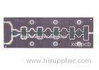

Advanced Microstrip Patch Antenna PCB Board With Taconic RF Base Material
| Place of Origin: | Zhejiang |
|---|
Company Profile
| Location: | Shenzhen, Guangdong, China (Mainland) |
|---|---|
| Business Type: | Manufacturer |
| Main Products: | Multilayer PCB, Fr4 PCB, High Frequency PCB |
Product Detail
| Model No.: | XCET |
|---|
Product Description
Advanced Microstrip Patch Antenna PCB Board With Taconic RF Base Material
Introduction:
The increasing complexity of electronic components and switches continually requires faster
signal flow rates, and thus higher transmission frequencies. Because of short pulse rise times
in electronic components, it has also become necessary for high frequency (HF) technology to
view conductor widths as an electronic component.
Depending on various parameters, HF signals are reflected on circuit board, meaning that the
impedance (dynamic resistance) varies with respect to the sending component. To prevent such
capacitive effects, all parameters must be exactly specified, and implemented with the highest level
of process control.
Critical for the impedances in high frequency circuit boards are principally the conductor trace
geometry,the layer buildup, and the dielectric constant (er) of the materials used.
Technology Sheet
| Capabilities | Standard Production | Advanced Production |
| Layer Count / Technology | 4 - 28 Layers | 4 - 28 Layers |
| PCB Thickness Range | 0.5 - 2.4 mm | 0.32 - 2.4 mm |
| Build Up | Core & Hybrid Build Up | Core & Hybrid Build Up |
| Materials | FR4 / Rogers / Taconic / others (Teflon based) |
FR4 / Taconic / Rogers / others on request |
| Glass Transition Temperature | 105 / 140/ 170 | 105/ 140/ 170 |
| Standard Glass Cloth | 106 / 1080 / 2116 / 1501 / 7628 |
1037 / 106 / 1080 / 2116 / 1501 / 7628 |
| Copper Thickness | 18μm / 35μm / 70μm |
9μm / 18μm / 35μm / 70μm |
| Copper Plating Holes | 20μm (25μm) | 13μm / 20μm/ 25μm |
| Min. Line / Spacing | 100μm / 100μm | 50μm / 50μm |
| Soldermask Registration | ‘+/- 65μm(Photoimageable) |
’+/- 25μm (Photoimageable) |
| Min. Soldermask Dam | 75μm | 60μm |
| Soldermask Color | Green / white / black / red / blue |
Green / white / black / red / blue |
| Max. PCB Size | 575 mm x 500 mm | 575 mm x 500 mm |
| Production Panel | 609.6 mm x 530 mm | 609.6 mm x 530 mm |

