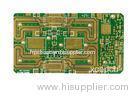

Turnkey Solar Inverter FR4 Multi Layer PCB Circuit Board With Design and Prototype Service
| Place of Origin: | Zhejiang |
|---|
Company Profile
| Location: | Shenzhen, Guangdong, China (Mainland) |
|---|---|
| Business Type: | Manufacturer |
| Main Products: | Multilayer PCB, Fr4 PCB, High Frequency PCB |
Product Detail
| Model No.: | XCEF |
|---|
Product Description
Turnkey Solar Inverter FR4 PCB Circuit Board With Design Service
Specification:
| Layers:2 | Material:FR4 |
| Board thickness:1.2MM | Copper thickness:1.5OZ |
| Min hole size:8mil | Min line space:8mil |
| Min line width:8mil | Surface:Lead free |
| Solder mask color: green | Certificate:Iso9001,SGS |
Parameter:
|
Copper thickness in hole |
>25.0 um (>1mil) |
|
Size |
Max. Board Size: 23 × 25 (580mm×900mm) |
|
Min. Drilled Hole Size: 3mil (0.075mm) |
|
|
Min. Line Width: 3mil (0.075mm) |
|
|
Min. Line Spacing: 3mil (0.075mm) |
|
|
Surface finishing |
HASL / HASL lead free, HAL, Chemical tin, Chemical Gold, Immersion Silver/Gold, OSP, Gold plating |
|
Tolerance
|
Shape tolerance: ±0.13 |
|
Hole tolerance: PTH: ±0.076 NPTH: ±0.05 |
|
|
Certificate |
UL, ISO 9001, ISO 14001 |
|
Special requirements |
Buried and blind vias+controlled impedance +BGA |
|
Profiling |
Punching, Routing, V-CUT, Beveling |
| Any other special material please feel free to let us know | |
Description:
Standard products(4, 6 layers), FR4, photo-sensitive soldermask
Special types (thick copper, thin core, hard gold, etc)
High layer count(8-40 layers)
High Density Interconnection (HDI): micro-via technology, build-up construction, laser holes, very small tracks, etc…
Low cost CPTH: polymer conductive holes with copper paste. 4 layers, FR4
Back panels: thick PCBs, press-fit technology, large size PCBs.


