
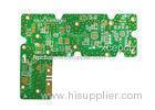

Multi-layer HF Rogers PCB Sufficient Material for Automotive Device 1OZ Double Layer PCB
| Place of Origin: | Zhejiang |
|---|
Company Profile
| Location: | Shenzhen, Guangdong, China (Mainland) |
|---|---|
| Business Type: | Manufacturer |
| Main Products: | Multilayer PCB, Fr4 PCB, High Frequency PCB |
Product Detail
| Model No.: | XCER-1 |
|---|
Product Description
Multi-layer HF Rogers PCB Sufficient Material In Automotive Device Application
Specification
- 2 layer
- Green solder mask,
- white silk screen
- Model:XCER
- Size: 15*9cm
- Location: Shenzhen
- Board thickness: 0.2mm
- Copper thickness: 1OZ
Laminates:
- High Tg, BT resins
- Low Dk, Low Df Formulations
- High Strength, Low CTE selections
- Polyimide/Kapton
- Multi-function FR-4
- Min Cladding 1 oz
- Max Cladding 2 oz
- Min Thickness .03mm (.0012)
Parameter
| Board thickness tolerance | T≥0.8mm±8%,T0.8mm±5% | ||||||||
| Wall hole copper thickness | 0.025mm(1mil) | ||||||||
| Finished hole | 0.2mm-6.3mm | ||||||||
| Min line width | 4mil/4mil(0.1/0.1mm) | ||||||||
| Min bonding pad space | 0.1mm(4mil) | ||||||||
| PTH aperture tolerance | ±0.075mm(3mil) | ||||||||
| NPTH aperture tolerance | ±0.05mm(2mil) | ||||||||
| Hole site deviation | ±0.05mm(2mil) | ||||||||
| Profile tolerance | ±0.10mm(4mil) | ||||||||
| Board bend&warp | ≤0.7% | ||||||||
| Insulation resistance | 1012Ωnormal | ||||||||
| Through-hole resistance | 300Ωnormal | ||||||||
| Electric strength | 1.3kv/mm | ||||||||
| Current breakdown | 10A | ||||||||
| Peel strength | 1.4N/mm | ||||||||
| Soldmask regidity | 6H | ||||||||
| Thermal stress | 28820Sec | ||||||||
| Testing voltage | 50-300v | ||||||||
| Min buried blind via | 0.2mm(8mil) | ||||||||
| Outer cooper thickness | 1oz-5oz | ||||||||
| Inner cooper thickness | 1/2 oz-4oz | ||||||||
| Aspect ratio | 8:1 | ||||||||
| SMT min green oil width | 0.08mm | ||||||||
| Min green oil open window | 0.05mm | ||||||||
| Insulation layer thickness | 0.075mm-5mm | ||||||||
| Aperture | 0.2mm-0.6mm | ||||||||
| Special technology | Inpedance,blind buried via,thick gold,aluminumPCB | ||||||||
| Surface finish | HASL,lead free,Immersion gold,immersion tin,immersion silver,ENIG,Blue glue,gold plating | ||||||||
Advantage:
Newest PCB machine and top technology,professional engineer team
Shorter PCB manufacturing lead times and improved device performance for Flip Chip, BGA, MCM, SIP technologies and medical devices.
Accept utilization of technologies that require ultra thin cores, fine line geometries and alternative via technologies for enhanced thermal transfer in the case of a thermal PCB.
Utilization of the technologies that require 20um circuit geometries, 30um dielectric layers, 50um laser vias and 125um bump pitch processing.