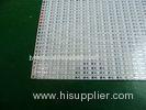

High Power SMD 3014 LED Panel PCB / Aluminum LED PCB Boards 1 Layer
| Place of Origin: | Zhejiang |
|---|
Company Profile
| Location: | Shenzhen, Guangdong, China (Mainland) |
|---|---|
| Business Type: | Manufacturer |
| Main Products: | Prototype PCB Boards, Double Sided PCB Board, 4 Layer PCB Prototype |
Product Detail
| Model No.: | JHD-LPP-1406 |
|---|
Product Description
High Power SMD 3014 LED Panel PCB / Aluminum LED PCB Boards 1 Layer
Professional PCB Manufacturing
Base Material: Aluminum
Layer: 1 layer
Board Thickness: 1.0mm/1.2mm/1.5mm/2.0mm/3.0mm
Board Dimension: Diameter 30mm,45mm,50mm,55mm,60mm,65mm(it can be customized)
Copper layer: 1oz/2oz/3oz
Solder Mask: White/Black/Blue/Red
Silkscreen: Black
Surface finish: LF HAL/HAL/OSP/Gold immersion/Silver plating
Outline Profile: CNC routing/V-Cut/Punching
All of the parameters can be customized!

Why us?
Quality
Our UL(E465880)/Rohs standards insure quality assemblies from start to finish. Whether it's a simple custom product or a complex turnkey production run, JHD PCB will adhere to the highest quality standards.
Capable
JHD PCB offers the latest in assembly capabilities and qualifications insuring that quality is built into every product we produce.
Experience
When it comes to your build you want a partner you can depend on. Our management team has over 8years of combined industry knowledge. Our engineering team has over 5 years experience.
Protecting your interests
Protecting your Intellectual Property is job one! Our staff of trained professionals are all working under a strict confidentiality contract and treat your important documentation as they would their own.
Flexibility
JHD PCB prides ourselves on our ability to custom tailor programs around our customers' needs. JHD PCB takes time to listen to your unique business needs and then set out to surpass them.
Lead Time
Samples: 3-4 days
Mass Production: 7-15 days(depend on the quantity)
Payment Terms
T/T,Western Union
Packing and Shipment
Vacuum package in carton

Factory Capability
|
Item |
Manufacturing Capability |
|
Surface Treatment |
OSP |
|
PCB Layer Type |
Single side,Double side |
|
Max. Working Panel Size |
1500mm*600mm |
|
Min. Working Panel Size |
4mm*4mm |
|
AL Substrate Thickness |
0.3mm-4mm |
|
Min. Conductor width |
0.15mm |
|
Min. Conductor spacing |
0.15mm |
|
Min. Drilling hole size |
0.2mm |
|
Plate Thickness Tolerance |
±0.1mm |
|
Finished Panel Tolerance |
±0.1mm |
|
V-CUT Alignment |
±0.1mm |
|
Hole Dia Tolerance |
±0.05mm |
|
Hole Position Tolerance |
±0.076mm |
|
Finished Copper Thickness |
35um-105um(1oz-6oz) |
|
Etching Under Cut |
>/=2.0 |
|
PTH&Panel Plating Uniformity |
>90% |
|
Eing/Flash Gold Thickness |
1-5u’’ |
|
Solder Mask Thickness |
15um-35um |
|
Min. Solder Mask Bridge |
0.076mm(3mil) |
|
Silk Screen |
White/Black(depend on your requirements) |
|
Thermal Conductivity |
1.0~20W/MK |
|
Withstand Voltage |
AC 2000V,DC 1500~4000V |
JHD PCB Company overview


JHD PCB in the professional lighting fair

Purchase Tips
a. If you want to purchase our PCB, you should provide a formal Gerber files or *.pcb file or something like that.
b. If you want to purchase by large quantity, please ask Mr.Hank.
c. If you want to purchase the PCBA, you should provide the Gerber files, *.pcb file , BOM list etc.
d. If you want to reproduce some exsited PCB board for you, please first provide very clear pictures , then if you are satisfied with our estimate quotation, then send us the real thing, so we can clone it for you.
e. If none of the above can help you, please contact us directly by Skype, QQ or Email. We are very glad to answer the questions you ask, your satisfaction is our final destination.
JHD PCB would like to be your reliable partner in near future!

