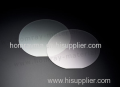
Homray Material Technology has established the manufacturing technology for free-standing Gallium Nitride wafer GaN substrate which is for UHB-LED and LD. Grown by hydride vapour phase epitaxy (HVPE) technology,Our GaN substrate has low defect density and less or free macro defect density.
Gallium nitride, GaN substrate. GaN has a wide direct bandgap, strong atomic bonds and high thermal conductivity, etc., and it is a strong ability on anti-radiation, Not only is the short-wavelength optoelectronic materials, Also the replacement materials of high temperature semiconductor device, GaN can be used to make blue and green LED, or violet, ultraviolet light LD, ultraviolet detectors and high-frequency high-power electronic devices.