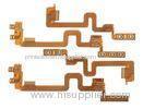

Flex Circuit Board 1 oz Copper Flexible PCB with0.15mm Thickness
| Place of Origin: | Zhejiang |
|---|
Company Profile
| Location: | Shenzhen, Guangdong, China (Mainland) |
|---|---|
| Business Type: | Manufacturer |
| Main Products: | PCB Board Assembly, Turnkey PCB Assembly, PCB Assembly Services |
Product Detail
| Model No.: | HSFPC1001 |
|---|
Product Description
Flexible PCB with best price/FPC supplier from shenzhen /FPC manufacturer, 0.15mm thickness 1oz
copper with immersion gold finish
Specification
1. Low Cost, High Quality flexible PCB board manufacturer
2. One-Stop Servie
3. OEM/ODM
4. Fast deliver 5-7 day
5. UL, RoHS, ISO
Detailed Specification of Flexible PCB Manufacturing
|
Technical Specification |
||
|
Layers: |
1~10 (flex Pcb) and 2~8 (rigid flex) |
|
|
Min Panel Size: |
5mm x 8mm |
|
|
Max Panel Size: |
250 x 520mm |
|
|
Min Finished board thickness: |
0.05mm (1 sided inclusive copper) |
|
|
Max Finished board thickness: |
0.3mm (2 sided inclusive copper) |
|
|
Finished board thickness tolerance: |
±0.02~0.03mm |
|
|
Material: |
Kapton, Polyimide, PET |
|
|
Base copper thickness (RA or ED): |
1/3 oz, 1/2 oz, 1oz, 2oz |
|
|
Base PI thickness: |
0.5mil, 0.7mil, 0.8mil, 1mil, 2mil |
|
|
Stiffner: |
Polyimide, PET, FR4, SUS |
|
|
Min Finished hole diameter: |
Φ 0.15mm |
|
|
Max Finished hole diameter: |
Φ 6.30mm |
|
|
Finished hole diameter tolerance (PTH): |
±2 mil ( ±0.050mm) |
|
|
Finished hole diameter tolerance (NPTH): |
±1 mil ( ±0.025mm) |
|
|
Min width/spacing (1/3oz): |
0.05mm/0.06mm |
|
|
Min width/spacing (1/2oz): |
0.06mm/0.07mm |
|
|
Min width/spacing (1oz): |
Single layer: 0.07mm/0.08mm |
|
|
Double layer: 0.08mm/0.09mm |
||
|
Aspect Ratio |
6:01 |
8:01 |
|
Base Copper |
1/3Oz--2Oz |
3 Oz for Prototype |
|
Size Tolerance |
Conductor Width:±10% |
W ≤0.5mm |
|
Hole Size: ±0.05mm |
H ≤1.5mm |
|
|
Hole Registration: ±0.050mm |
||
|
Outline Tolerance:±0.075mm |
L ≤50mm |
|
|
Surface Treatment |
ENIG: 0.025um - 3um |
|
|
OSP: |
||
|
Immersion Tin: 0.04-1.5um |
||
|
Dielectric Strength |
AC500V |
|
|
Solder Float |
288/10s |
IPC Standard |
|
Peeling Strength |
1.0kgf/cm |
IPC-TM-650 |
|
Flammability |
94V-O |
UL94 |
Welcome to Huaswin!
Huaswin Electronics is a professional PCB & PCB Assembly manufacturer, located in Shenzhen, China.
We supply one-stop facility services: PCB design, PCB fabrication, components procurement, SMT and DIP
assembly ,IC pre-programming / burning on-line, testing, anti-static packing.
PCB capability and services:
1. Single-sided, double-sided & multi-layer PCB (up to 30 layers)
2. Flexible PCB (up to 10 layers)
3. Rigid-flex PCB (up to 8 layers)
4. CEM-1, CEM-3 FR-4, FR-4 High TG, Polyimide, Aluminum-based material.
5. HAL, HAL lead free, Immersion Gold/ Silver/Tin, Hard Gold, OSP surface treatment.
6. Printed Circuit Boards are 94V0 compliant, and adhere to IPC610 Class 2 international PCB standard.
7. Quantities range from prototype to volume production.
8. 100% E-Test
PCB Assembly services:
SMT Assembly
Automatic Pick & Place
Component Placement as Small as 0201
Fine Pitch QEP - BGA
Automatic Optical Inspection
Through-hole Assembly
Wave Soldering
Hand Assembly and Soldering
Material Sourcing
IC pre-programming / Burning on-line
Function testing as requested
Aging test for LED and Power boards
Complete unit assembly (which including plastics, metal box, Coil, cable assembly etc)
Packing design
Conformal coating
Both dip-coating and vertical spray coating is available. Protecting non-conductive dielectric layer that is
applied onto the printed circuit board assembly to protect the electronic assembly from damage due to
contamination, salt spray, moisture, fungus, dust and corrosion caused by harsh or extreme environments.
When coated, it is clearly visible as a clear and shiny material.
Complete box build
Complete 'Box Build' solutions including materials management of all components, electromechanical parts,
plastics, casings and print & packaging material
Testing Methods
AOI Testing
· Checks for solder paste
· Checks for components down to 0201"
· Checks for missing components, offset, incorrect parts, polarity
X-Ray Inspection
X-Ray provides high-resolution inspection of:
· BGAs
· Bare boards
In-Circuit Testing
In-Circuit Testing is commonly used in conjunction with AOI minimizing functional defects caused by
component problems.
· Power-up Test
&m

