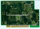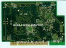

Stacked Via Impedance 4 Layer PCB Printed Circuit Board Tg 180 White Silkscreen
| Place of Origin: | Zhejiang |
|---|
Company Profile
| Location: | Shenzhen, Guangdong, China (Mainland) |
|---|---|
| Business Type: | Manufacturer |
| Main Products: | Multi Layer PCB, Custom PCB Boards, PCB Printed Circuit Board |
Product Detail
| Model No.: | SYF-050 |
|---|
Product Description
Stacked Via Impedance 4 Layer PCB Printed Circuit Board Tg 180 White Silkscreen
|
PRODUCT’S DETAILS |
|
|
Raw Material |
FR-4 (Tg 180 available) |
|
Layer Count |
4-Layer |
|
Board Thickness |
2.0mm |
|
Copper Thickness |
2.0oz |
|
Surface Finish |
ENIG(Electroless Nickel Immersion Gold) |
|
Solder Mask |
Green |
|
Silkscreen |
White |
|
Min. Trace Width/Spacing |
0.075/0.075mm |
|
Min. Hole Size |
0.25mm |
|
Hole Wall Copper Thickness |
≥20μm |
|
Measurement |
300×400mm |
|
Packaging |
Inner: Vacuum-packed in soft plastic bales |
|
Application |
Communication,automobile,cell,computer,medical |
|
Advantage |
Competitive Price,Fast Delivery,OEM&ODM,Free Samples, |
|
Special Requirements |
Buried And Blind Via, Impedance Control, Via Plug, |
|
Certification |
UL,ISO9001:2008,ROHS,REACH,SGS,HALOGEN-FREE |
|
PRODUCTION CAPABILITY OF PCB |
||
|
|
ITEMS Item |
|
|
Laminate |
Type |
FR-1,FR-5,FR-4 High-Tg,ROGERS,ISOLA,ITEQ, |
|
Thickness |
0.23.2mm |
|
|
Production Type |
Layer Count |
2L-16L |
|
Surface Treatment |
HAL,Gold Plating,Immersion Gold,OSP, |
|
|
Cut Lamination |
Max. Working Panel size |
1000×1200mm |
|
Inner Layer |
Internal Core Thickness |
0.12.0mm |
|
Internal width/spacing |
Min: 4/4mil |
|
|
Internal Copper Thickness |
1.0~3.0oz |
|
|
Dimension |
Board Thickness Tolerance |
±10% |
|
Interlayer Alignment |
±3mil |
|