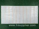

SMD3528 / 5050 Custom LED Strip PCB with White / Black Solder Mask 1 layer / 2 layer
| Place of Origin: | Zhejiang |
|---|
Company Profile
| Location: | Shenzhen, Guangdong, China (Mainland) |
|---|---|
| Business Type: | Manufacturer |
| Main Products: | LED Light PCB, LED Tube PCB, LED Bulb PCB |
Product Detail
| Model No.: | JHD-SP-1407 |
|---|
Product Description
SMD3528 / 5050 Custom LED Strip PCB with White / Black Solder Mask 1 layer / 2 layer
Professional PCB Manufacturing
Base Material: Polyimide
Layer: 1 layer/2 layers
Board Thickness: 0.1-0.3mm
Board Dimension: 500x8mm,500x10mm,500x12mm
Copper layer: 15um,18um,25um,35um
Solder Mask: White/Black
Silkscreen: Black
Surface finish: OSP/Gold immersion
Outline Profile: Punching
All of the parameters can be customized!

Features for led strip pcb:
1.Wide applicability, easy to install and maintain
2. Extremely luminous, with wide viewing angle,perfect angle is 120
3. PC base board, unique waterproof technique
4. Energy saving and environmental friendly,No UV or RF interference ,no Mercury or led
5. Operating low voltage DC 12V for human safety
6. Various colors are available
7. Very bright,low power consumption
8. Cuttable every 3 SMD LEDs
9. Long lifespan: More than 50, 000 hours
Safety and Maintenance Information
1.SMD LED ribbon itself and all its components may not be mechanically stressed.
2.Don't damage or destroy conducting paths on the curcuit board while installation.
3.To guarantee safety,only qualified person are allowed to install led strips.
4.Make sure SMD LED ribbons are mounted to correct electrical polarity.
5.Parallel connection is highly recommended for its high safety.
6.Serial connection is not recommended because unbalanced voltage drop may damage SMD LED strips
7.Insufficient and unstable power supply may cause flexible strip damage.
8.Don't install SMD ribbons dicectly on metallic or any other conductive surfaces.
Lead Time
Samples: 3-4 days
Mass Production: 7-18 days(depend on the quantity)
Payment Terms
T/T,Western Union
Packing and Shipment
Vacuum package in carton

Factory Capability
|
Item |
Manufacturing Capability |
|
Surface Treatment |
OSP |
|
PCB Layer Type |
Single side,Double side |
|
Max. Working Panel Size |
1500mm*600mm |
|
Min. Working Panel Size |
4mm*4mm |
|
AL Substrate Thickness |
0.3mm-4mm |
|
Min. Conductor width |
0.15mm |
|
Min. Conductor spacing |
0.15mm |
|
Min. Drilling hole size |
0.2mm |
|
Plate Thickness Tolerance |
±0.1mm |
|
Finished Panel Tolerance |
±0.1mm |
|
V-CUT Alignment |
±0.1mm |
|
Hole Dia Tolerance |
±0.05mm |
|
Hole Position Tolerance |
±0.076mm |
|
Finished Copper Thickness |
35um-105um(1oz-6oz) |
|
Etching Under Cut |
>/=2.0 |
|
PTH&Panel Plating Uniformity |
>90% |
|
Eing/Flash Gold Thickness |
1-5u’’ |
|
Solder Mask Thickness |
15um-35um |
|
Min. Solder Mask Bridge |
0.076mm(3mil) |
|
Silk Screen |
White/Black(depend on your requirements) |
|
Thermal Conductivity |
1.0~20W/MK |
|
Withstand Voltage |
AC 2000V,DC 1500~4000V |
JHD PCB Company overview


JHD PCB in the professional lighting fair

Purchase Tips
a. If you want to purchase our PCB, you should provide a formal Gerber files or *.pcb file or something like that.
b. If you want to purchase by large quantity, please ask by SQM.
c. If you want to purchase the PCBA, you should provide the Gerber files, *.pcb file , BOM list etc.
d. If you want to reproduce some exsited PCB board for you, please first provide very clear pictures , then if you are satisfied with our estimate quotation, then send us the real thing, so we can clone it for you.
e. If none of the above can help you, please contact us directly by Skype, QQ or Email. We are very glad to answer the questions you ask, your satisfaction is our final destination.
JHD PCB would like to be your reliable partner in near future!


