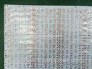

SMD DC 12V / 24V LED Strip PCB Board
| Place of Origin: | Zhejiang |
|---|
Company Profile
| Location: | Shenzhen, Guangdong, China (Mainland) |
|---|---|
| Business Type: | Manufacturer |
| Main Products: | LED Light PCB, LED Tube PCB, LED Bulb PCB |
Product Detail
| Model No.: | JHD-SP-1404 |
|---|
Product Description
Professional PCB Manufacturing
Base Material: Polyimide
Layer: 1 layer/2 layers
Board Thickness: 0.1-0.3mm
Board Dimension: 500x8mm,500x10mm,500x12mm
Copper layer: 15um,18um,25um,35um
Solder Mask: White/Black
Silkscreen: Black
Surface finish: OSP/Gold immersion
Outline Profile: Punching
All of the parameters can be customized!

Led Strip PCB Applications:
1.car decoration
2.Architectural decorative lighting
3.Archway, canopy and bridge edge lighting
4.Amusement park,theater and aircraf cabin mood lighting
5.Emergency walkway lighting
6.Stairway accent lighting
7.Backlighting for signage letters
8.Channel letter lighting
9.Cove lighting
LED strip PCB Feature
*High efficiency and high intensity
*Super bright SMD, Easy installation
*Green Products , Energy saving and Low power Consumption
*Competitive prices,stable quality short lead time
*No fluorescent flickering, No RF Interference and No buzzing Noise
*CE/ROHS Certification
*Environment friendly and rich color
Advantages
1. Non-waterproof
IP65 Waterproof (Epoxy cover waterproof, Epoxy Resin)
IP67 Waterproof (Silicon sleeve waterproof )
IP68 Waterproof (Fully waterproof plastic irrigation)
2. Golden and White PCB color or customer required
3. 3M adhesive tape on its back
4. NO flickering, No RF interference and NO UV radiation
5. CE& ROHS approved
6. Safety, energy conservation and environmental protection
7. Reflow soldering and SMT technology.
8. Flexible and can corner paste
9. Fast response and can shine in microseconds
Lead Time
Samples: 3-4 days
Mass Production: 7-15 days(depend on the quantity)
Payment Terms
T/T,Western Union
Packing and Shipment
Vacuum package in carton

Factory Capability
|
Item |
Manufacturing Capability |
|
Surface Treatment |
OSP |
|
PCB Layer Type |
Single side,Double side |
|
Max. Working Panel Size |
1500mm*600mm |
|
Min. Working Panel Size |
4mm*4mm |
|
AL Substrate Thickness |
0.3mm-4mm |
|
Min. Conductor width |
0.15mm |
|
Min. Conductor spacing |
0.15mm |
|
Min. Drilling hole size |
0.2mm |
|
Plate Thickness Tolerance |
±0.1mm |
|
Finished Panel Tolerance |
±0.1mm |
|
V-CUT Alignment |
±0.1mm |
|
Hole Dia Tolerance |
±0.05mm |
|
Hole Position Tolerance |
±0.076mm |
|
Finished Copper Thickness |
35um-105um(1oz-6oz) |
|
Etching Under Cut |
>/=2.0 |
|
PTH&Panel Plating Uniformity |
>90% |
|
Eing/Flash Gold Thickness |
1-5u’’ |
|
Solder Mask Thickness |
15um-35um |
|
Min. Solder Mask Bridge |
0.076mm(3mil) |
|
Silk Screen |
White/Black(depend on your requirements) |
|
Thermal Conductivity |
1.0~20W/MK |
|
Withstand Voltage |
AC 2000V,DC 1500~4000V |
JHD PCB Company overview


JHD PCB in the professional lighting fair

Purchase Tips
a. If you want to purchase our PCB, you should provide a formal Gerber files or *.pcb file or something like that.
b. If you want to purchase by large quantity, please ask by SQM.
c. If you want to purchase the PCBA, you should provide the Gerber files, *.pcb file , BOM list etc.
d. If you want to reproduce some exsited PCB board for you, please first provide very clear pictures , then if you are satisfied with our estimate quotation, then send us the real thing, so we can clone it for you.
e. If none of the above can help you, please contact us directly by Skype, QQ or Email. We are very glad to answer the questions you ask, your satisfaction is our final destination.
JHD PCB would like to be your reliable partner in near future!

