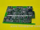
Multilayer 4 Layer OSP Lead Free PCB FR4 , TG135 / 1.6mm Board Thickness
| Place of Origin: | Zhejiang |
|---|
Company Profile
| Location: | Shenzhen, Guangdong, China (Mainland) |
|---|---|
| Business Type: | Manufacturer, Distributor/Wholesaler |
| Main Products: | Double Sided PCB |
Product Description
Multilayer 4 Layer OSP Lead Free PCB FR4 , TG135 / 1.6mm Board Thickness
Specifications
1.Export PCB many years
2. Fast service delivery
3. UL,SGS,ROHS,ISO9001
4.Professional production tech
We manufacture Multi-layer PCB: High quality with low price (Good tolerance, Good warpage, Good solder mask...)
The information about our company's process capacity for your reference:
|
Item |
Capability |
|||
|
1.Base Material |
FR-4 / High TG FR-4 / Lead free Materials (ROHS Compliant) / Halogen Free material /CEM-3/CEM-1/ /PTFE/ROGERS/ARLON/TACONIC |
|||
|
2.Layers |
1-30 |
|||
|
3.Finised inner/outer copper thickness |
1-12OZ |
|||
|
4.Finished board thickness |
0.2-7.0mm |
|||
|
Tolerance |
Board thickness≤1.0mm: +/-0.1mm 1<Board thickness≤2.0mm: +/-10% Board thickness>2.0mm: +/-8% |
|||
|
5.Max panel size |
≤2sidesPCB: 600*1500mm Multilayer PCB: 500*1200mm |
|||
|
6.Min conductor line width/spacing |
Inner layers: ≥3/3mil Outer layers: ≥3.5/3.5mil |
|||
|
7.Min hole size |
Mechanical hole: 0.15mm Laser hole: 0.1mm |
|||
|
Drilling precision: first drilling |
First drilling: 1mil Second drilling: 4mil |
|||
|
8.Warpage |
Board thickness≤0.79mm: β≤1.0% 0.80≤Board thickness≤2.4mm: β≤0.7% Board thickness≥2.5mm: β≤0.5% |
|||
|
9.Controlled Impedance |
+/-5% |
|||
|
10. Aspect Ratio |
15:1 |
|||
|
11.Min welding ring |
4mil |
|||
|
12.Min solder mask bridge |
≥0.08mm |
|||
|
13.Plugging vias capability |
0.2-0.8mm |
|||
|
14. Hole tolerance |
PTH: +/-3mil NPTH: +/-2mil |
|||
|
15.Outline profile |
Rout/ V-cut/ Bridge/ Stamp hole |
|||

