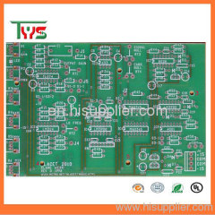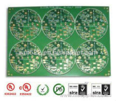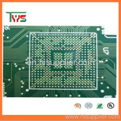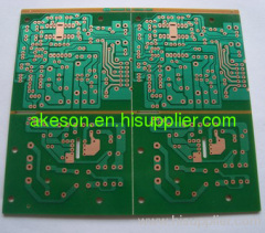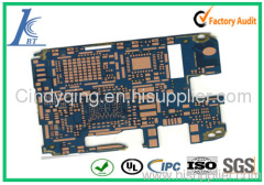
Green color single sided pcb
| Place of Origin: | Zhejiang |
|---|
Company Profile
| Location: | Shenzhen, Guangdong, China (Mainland) |
|---|---|
| Business Type: | Manufacturer, Distributor/Wholesaler |
| Main Products: | Double Sided PCB |
Product Description
Green color single sided pcb
Specifications
2.High layers PCB manufacturing, up to 32 layers
3.High Quality and best servise
4.No MOQ
Our Goal:To provide you with the best service and the best quality !
Detailed Specification of PCB And PCBA Manufacturing
|
Item |
Capability |
|
|
1.Base Material |
FR-4 / High TG FR-4 / Lead free Materials (ROHS Compliant) / Halogen Free material /CEM-3/CEM-1/ /PTFE/ROGERS/ARLON/TACONIC |
|
|
2.Layers |
1-30 |
|
|
3.Finised inner/outer copper thickness |
1-12OZ |
|
|
4.Finished board thickness |
0.2-7.0mm |
|
|
Tolerance |
Board thickness≤1.0mm: +/-0.1mm 1<Board thickness≤2.0mm: +/-10% Board thickness>2.0mm: +/-8% |
|
|
5.Max panel size |
≤2sidesPCB: 600*1500mm Multilayer PCB: 500*1200mm |
|
|
6.Min conductor line width/spacing |
Inner layers: ≥3/3mil Outer layers: ≥3.5/3.5mil |
|
|
7.Min hole size |
Mechanical hole: 0.15mm Laser hole: 0.1mm |
|
|
Drilling precision: first drilling |
First drilling: 1mil Second drilling: 4mil |
|
|
8.Warpage |
Board thickness≤0.79mm: β≤1.0% 0.80≤Board thickness≤2.4mm: β≤0.7% Board thickness≥2.5mm: β≤0.5% |
|
|
9.Controlled Impedance |
+/-5% |
|
|
10. Aspect Ratio |
15:1 |
|
|
11.Min welding ring |
4mil |
|
|
12.Min solder mask bridge |
≥0.08mm |
|
|
13.Plugging vias capability |
0.2-0.8mm |
|
|
14. Hole tolerance |
PTH: +/-3mil NPTH: +/-2mil |
|
|
15.Outline profile |
Rout/ V-cut/ Bridge/ Stamp hole |
|
|
16.Surface treatment |
OSP: 0.5-0.5um HASL: 2-40um Lead free HASL: 2-40um
| |


