
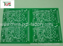
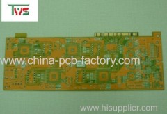
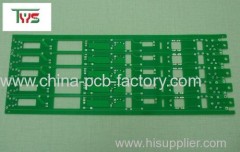
Fr4 PCB / immersion Tin Silver ENIG / HASL
| Min. Order: | 10 PCS |
|---|---|
| Trade Term: | FOB |
| Payment Terms: | L/C, T/T, WU, payple |
| Supply Ability: | 12000pcs/mouth |
| Place of Origin: | Guangdong |
Company Profile
| Location: | Shenzhen, Guangdong, China (Mainland) |
|---|---|
| Business Type: | Manufacturer |
| Main Products: | PCB |
Product Detail
| Model No.: | tws-pll-2013112605 |
|---|---|
| Means of Transport: | Ocean, Air, Land |
| Brand Name: | TWS |
| Base Material: | aluminum /fr4/94v0/fpc/cem-1/cem-3 |
| Copper Thickness: | 0.2-2OZ |
| Board Thickness: | 0.2-4mm |
| Min. Hole Size: | 0.2mm |
| Min. Line Width: | 0.1mm |
| Min. Line Spacing: | 0.1mm |
| Surface Finishing: | HASL/OSP |
| Production Capacity: | 12000pcs/mouth |
| Packing: | vacuum package + caton box |
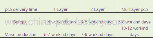
| Delivery Date: | 5-15days |
Product Description
NO | Item | Craft Capacity |
1 | Layer | 1-28 Layers |
2 | Base Material for PCB | FR4, CEM-1, TACONIC, Aluminium, High Tg Material, High Frequence ROGERS ,TEFLON, ARLON, Halogen-free Material |
3 | Rang of finish baords Thickness | 0.1-4.0mm |
4 | Max size of finish board | 900MM*900MM |
5 | Minimum Linewidth | 3mil (0.075mm) |
6 | Minimum Line space | 3mil (0.075mm) |
7 | Min space between pad to pad | 3mil (0.075mm) |
8 | Minimum hole diameter | 0.10 mm |
9 | Min bonding pad diameter | 10mil |
10 | Max proportion of drilling hole and board thickness | 1:12.5 |
11 | Minimum linewidth of Idents | 4mil |
12 | Min Height of Idents | 25mil |
13 | Finishing Treatment | HASL (Tin-Lead Free), ENIG(Immersion Gold), Immersion Silver , Gold Plating (Flash Gold), OSP, etc. |
14 | Soldermask | Green, White, Red, Yellow, Black, Blue, transparent photosensitive soldermask, Strippable soldermask. |
15 | Minimun thickness of soldermask | 10um |
16 | Color of silk-screen | White, Black, Yellow ect. |
17 | E-Testing | 100% E-Testing (High Voltage Testing); Flying Probe Testing |
18 | Other test | ImpedanceTesting,Resistance Testing, Microsection etc., |
19 | Date file format | GERBER FILE and DRILLING FILE, PROTEL SERIES, PADS2000 SERIES, Powerpcb SERIES, ODB++ |
20 | Special technological requirement | Blind & Buried Vias and High Thickness copper |
21 | Thickness of Copper | 0.5-14oz (18-490um) |
Factory inspection flow chart:

Advaced production equipment:


Our delivery time:
About factory
1.Experience: we have 20 years experinecs in circuit board manufacturing,with 50 employees and 60 excellent engineers, covering an area of 13000 square meters.Monthly capability is more than 5000 square meters, 4500 types/month. we cooperate with some well-known enterprises, such as Panasonic, HP,Honeywell and so on.
2.anything wrong happening in our products will be solved within 2 hours. we always offer relative technical support/consultant. Quick response. all your inquiry will be replied within 24 hours.
3. Our products and service are sold well in North America, West Europe, Japan, Singpore, Malaysia and other countries.


Meet your need is our greatest pursuit .If you are looking for a pcb board manufacturer in china,Please give us your files of pcb for a quote (Gerber files and specification), I will reply email in 3 hours. You also can contact us by .