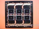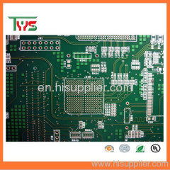

pcb circuit for High Frequency Devices
57.0~200.0 USD
| Min. Order: | 1 Square Meter |
|---|---|
| Trade Term: | FOB |
| Payment Terms: | T/T |
| Supply Ability: | 1000square meter/per day |
| Place of Origin: | Guangdong |
Company Profile
| Location: | Shenzhen, Guangdong, China (Mainland) |
|---|---|
| Business Type: | Manufacturer |
| Main Products: | PCB |
Product Detail
| Model No.: | 532Z |
|---|---|
| Max pane size: | 14"*20" |
| Independence tolerance: | +/-10% |
| Aspecr Ratio: | 9:1 |
| Layer count: | 1-20 |
| Solder mask abrasion: | ≥8H |
| Gold finger: | Ni: 80~250u", Au: 1~5u" |
| Warp and twist: | ≤0.75% |
| Via plug: | Max via size: 24mil (0.6mm) |
| Peel Strength: | 1.4N/mm |
| Certification: | UL/SGS/ROHS |
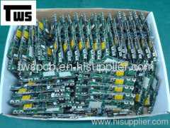
| Production Capacity: | 1000square meter/per day |
| Packing: | Inner vacuum and plastic package,outer carton box package |
| Delivery Date: | 3~10days |
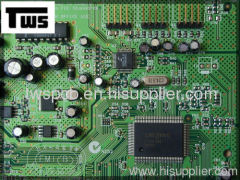
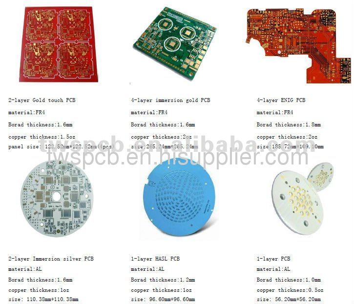
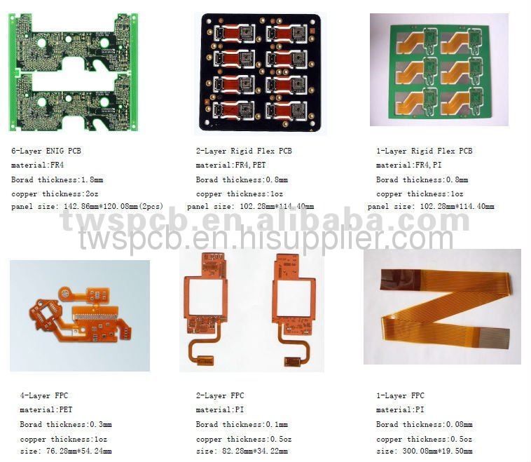
Product Description
Quick Details
| Place ofOrigin: | Japan | Number ofLayers: | 1-16 Layer | BaseMaterial: | FR-5/BT etc |
| Copper Thickness: | 0.018mm/0.035mm/0.070mm etc | Board Thickness: | 0.1-3.0mm | Min. Hole Size: | 0.15mm |
| Min. Line Width: | 0.05mm | Min. Line Spacing: | 0.05mm | Surface Finishing: | Gold/Silver etc |
Packaging & Delivery
| Packaging Detail: | standeard export packaging |
| Delivery Detail: | about 3 weeks |
Specifications
1.Milling-out Technology
2.High Frequency Devices
3.Gold plating
4.Glass Epoxy
2.High Frequency Devices
3.Gold plating
4.Glass Epoxy
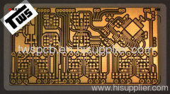
Module PCB for High FrequencyDevices
Specific processing technology is applied to the material and itenables to provide high
density, thinner dielectric PCB required forcommunication apparatus.
Specific processing technology is applied to the material and itenables to provide high
density, thinner dielectric PCB required forcommunication apparatus.
•KEYTECHNOLOGY
| FA & Robot | Automobile | Medical & Sensing | LED | Chip size Package | High Frequency Module | Chip on Board | BGA | Multi Chip Module | |
| Inner Layer Milling Technology | A | B | A | B | A | A | A | A | A |
| High Dam Printing Technology | A | B | A | B | A | A | A | A | A |
| Laser via Technology | A | B | A | B | A | A | A | A | A |
| Stacking Technology | A | B | A | A | B | A | B | A | A |
| Electroless Soft Gold plating Technology | A | A | A | A | A | A | A | A | A |
| Pin Caulking Technology | B | B | A | B | B | A | B | A | B |
| Dry Film Tent on Via Technology | B | B | B | A | A | B | A | B | B |
| Punching Technology | B | B | B | A | B | A | B | B | A |
| Flat Push Back Technology | A | A | A | A | B | A | B | B | A |
•CAPABILITIES
Panel size =340x340mm
406x340mm
510x340mm
Thickness =0.06-3.0mm
Material = Hitachi,Mitsubishi, Matsushita,
Risho,Kyocera, Rogers
Capacity = 10,000m²/monthover
Products = Dual sidePCB
Multi-layer PCB(3-16 layers)
Build-up PCB
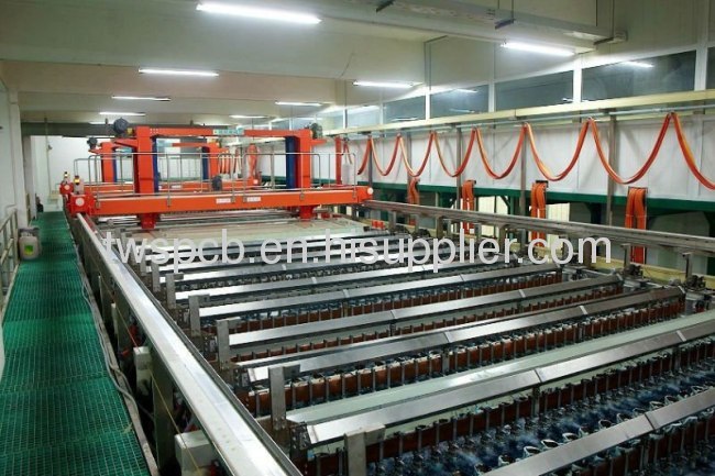
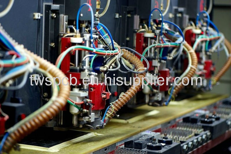
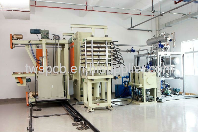
Advanced ProductionEquipment
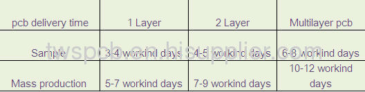
Our deliverytime:
Product HighQuality Perfect
Our deliverytime:
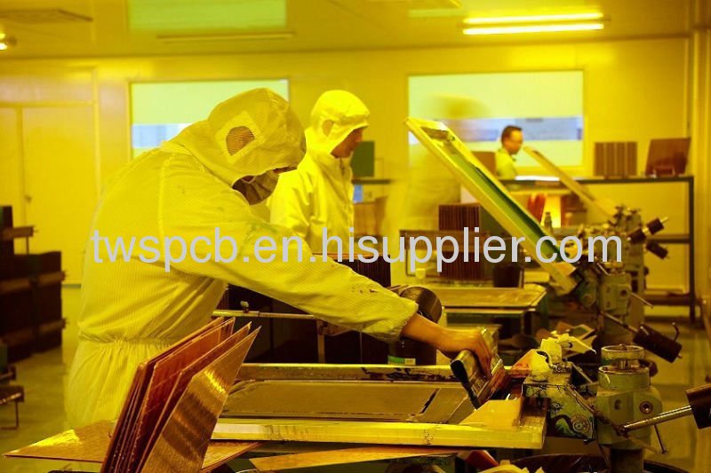
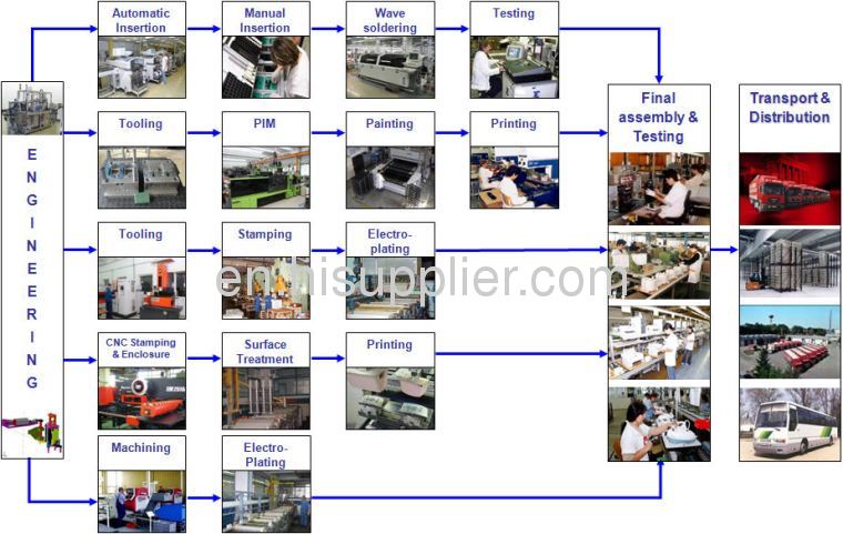
1.About Factory:
Experience: we have 20 years experinecsin circuit board manufacturing,with 50 employees and 60 excellent engineers,covering an area of 13000 square meters.Monthly capability is more than 5000square meters, 4500 types/month. we cooperate with some well-known enterprises,such as Panasonic, HP,Honeywell and so on.
2.Good after sales service:
anything wrong happening in our products willbe solved within 2 hours. we always offer relative technical support/consultant.Quick response. all your inquiry will be replied within 24 hours.
3.Ourproducts and service are sold well in North America,West Europe, Japan,Singpore, Malaysia and other countries.
Meet your need is ourgreatest pursuit .If you are looking for a pcb board manufacturerinchina,Pleasegive us your files ofpcb for a quote (Gerberfiles and specification),I will reply email in 3hours. Youalso cancontact usby .
1.Advanced production lines andprofessional staff.
2.Honesty credibility in china'stop.
3.Competest price but highquality.
4. One-stopservice.
5.Delivery ontime.
.jpg)