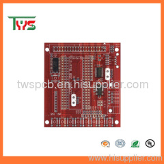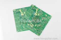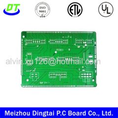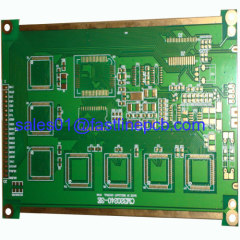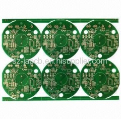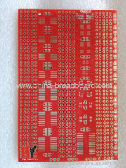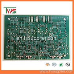

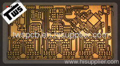
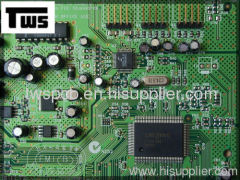
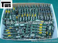
High quality double Layer PCB board
57.0~200.0 USD
| Min. Order: | 1 Square Meter |
|---|---|
| Trade Term: | FOB |
| Payment Terms: | L/C, D/A, T/T |
| Supply Ability: | 1000square meter/per day |
| Place of Origin: | Guangdong |
Company Profile
| Location: | Shenzhen, Guangdong, China (Mainland) |
|---|---|
| Business Type: | Manufacturer |
| Main Products: | PCB |
Product Detail
| Model No.: | KOIL3650 |
|---|---|
| Means of Transport: | Ocean |
| Max pane size: | 14"*20" |
| Independence tolerance: | +/-10% |
| Aspecr Ratio: | 9:1 |
| Layer count: | 1-20 |
| Solder mask abrasion: | ≥8H |
| Gold finger: | Ni: 80~250u", Au: 1~5u" |
| Warp and twist: | ≤0.75% |
| Via plug: | Max via size: 24mil (0.6mm) |
| Peel Strength: | 1.4N/mm |
| Certification: | UL/SGS/ROHS |
| Production Capacity: | 1000square meter/per day |
| Packing: | Inner vacuum and plastic package,outer carton box package |
| Delivery Date: | 3~10days |
Product Description
Quick Details
| Place ofOrigin: | Guangdong China (Mainland) | BrandName: | Eastwin | ModelNumber: | EW30306Y119 |
| Base Material: | FR-4 | Copper Thickness: | 1oz | Board Thickness: | 1.6mm |
| Min. Hole Size: | 0.1mm | Min. Line Width: | 0.1mm | Min. Line Spacing: | 0.1mm |
| Surface Finishing: | HASL | Item Name: | double Layer PCB board | Solder Mask: | red,white,black,blue,yellow |
| Silk Screen: | Silver,white,yellow | Design File Formate: | Gerber RS-274,274D,Eagleand AutoCAD's DXF,DWG | V-Score Depth: | 20-25% of board thickness |
Packaging & Delivery
| Packaging Detail: | Inner packing :Vacuum Package Outer packing:Standard Carton |
| Delivery Detail: | PCB:5-7 days pcba:20-25 days |
Specifications
1.double Layer pcb
2.FR4,UL&ROHSApproval,100%E-tested
3.OEM&OEM pcb board
4.Cost effectivemanufacture of double layer pcb
2.FR4,UL&ROHSApproval,100%E-tested
3.OEM&OEM pcb board
4.Cost effectivemanufacture of double layer pcb
High quality double Layer PCBboard
Welcome toEastwin!
PCB processcapability:
1.Layer:2-22 layer
2.Product type:RigidPCB,High Density Inverter PCB,thick copper PCB
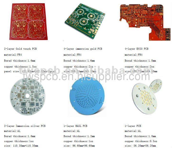
3.Materials:FR-4, CEM-3,Teflon, Aluminum Substrate, Rogers, Halogen Free, High Tg
4.CopperThickness:140micron(4oz)
5.Min Board Thickness:0.4mm
6.Max BoardThickness:5.0mm
7.Min finished Hole Diameter:0.1mm
8.Outer layer linewidth / spacing:0.1mm/0.1mm
9.Inner layer line width / spacing: 0.1mm/0.1mm
10.Min aperture:0.2mm
11.Min Laser drilling: 0.1mm
12.MinRing Width:0.11mm
13.Min BGA-bit hole spacing: 0.4mm
14.Resistance Tolerance:±10%
15.Minimum Insulation Thickness: 3mil
16.Maximum laser blind hole thickness to diameter ratio: 0.8:1
17.Maximum working board size:520*622mm
18.Drilling Tolerance(PTH):±0.075mm
19.Drilling tolerance (NPTH): ±0.05mm
20.OutlineTolerance (CNC): ±0.13mm
21.Surface coating:Lead Free HAL, HAL, FlashGold, Immersion Gold, Immersion Tin, Immersion Silver, OSP, Gold Finger Plating,Carbon Ink Printing, Peelable Blue Mask
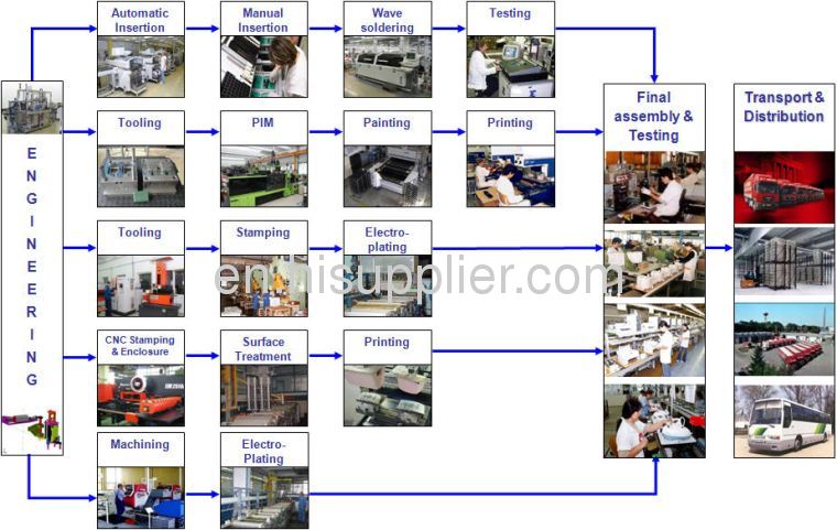
Your single point of contact for all ofyour raw materials, parts, and pcb assembly,also offers:
-Contract Manufacturing
- Engineering Services
- PCB Design &Assembly
- Product Design
- Prototyping
- Cable and WireAssemblies
- Plastics and Molds
-Contract Manufacturing
- Engineering Services
- PCB Design &Assembly
- Product Design
- Prototyping
- Cable and WireAssemblies
- Plastics and Molds
Detailed Terms for PcbAssembly
Technicalrequirement:
1) Professional Surface-mounting andThrough-hole soldering Technology
2) Various sizes like 1206,0805,0603components SMT technology
3) ICT(In Circuit Test),FCT(Functional CircuitTest) technology.
4) PCB Assembly With UL,CE,FCC,Rohs Approval
5) Nitrogengas reflow soldering technology for SMT.
6) High Standard SMT&SolderAssembly Line
7) High density interconnected board placement technologycapacity.
Quoterequirement:
1)Gerber file and Bomlist
2)Clear pics of pcba or pcba sample for us
3)Test method for PCBA
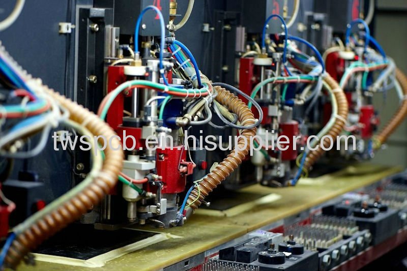
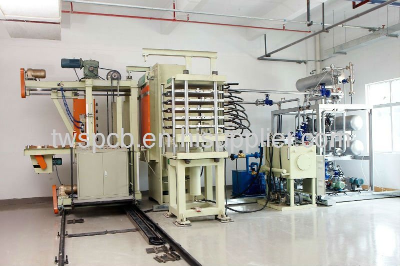
Advanced ProductionEquipment
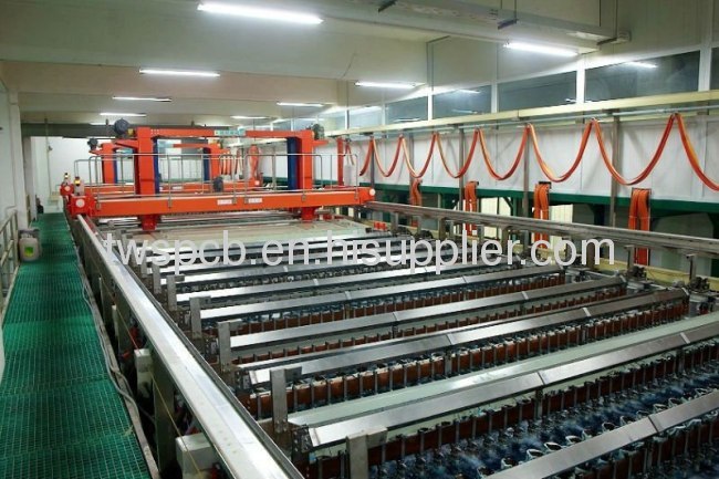
Our deliverytime:

1)Gerber file and Bomlist
2)Clear pics of pcba or pcba sample for us
3)Test method for PCBA
Advanced ProductionEquipment


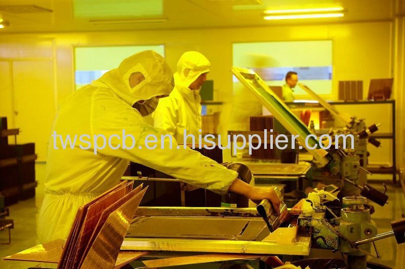
Product HighQuality Perfect


Our deliverytime:

1.About Factory:
Experience: we have 20 years experinecsin circuit board manufacturing,with 50 employees and 60 excellent engineers,covering an area of 13000 square meters.Monthly capability is more than 5000square meters, 4500 types/month. we cooperate with some well-known enterprises,such as Panasonic, HP,Honeywell and so on.
2.Good after sales service:
anything wrong happening in our products willbe solved within 2 hours. we always offer relative technical support/consultant.Quick response. all your inquiry will be replied within 24 hours.
3.Ourproducts and service are sold well in North America,West Europe, Japan,Singpore, Malaysia and other countries.


Meet your need is ourgreatest pursuit .If you are looking for a pcb board manufacturerinchina,Pleasegive us your files ofpcb for a quote (Gerberfiles and specification),I will reply email in 3hours. Youalso cancontact usby .
1.Advanced production lines andprofessional staff.
2.Honesty credibility in china'stop.
3.Competest price but highquality.
4. One-stopservice.
5.Delivery ontime.
