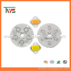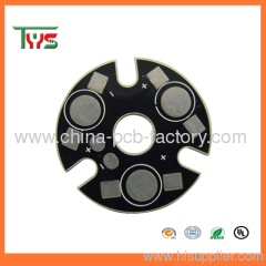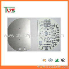
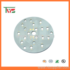
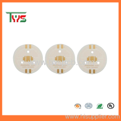
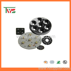
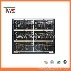
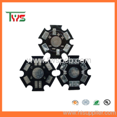
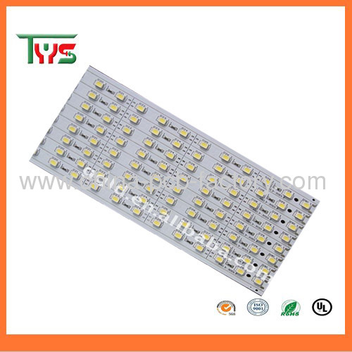
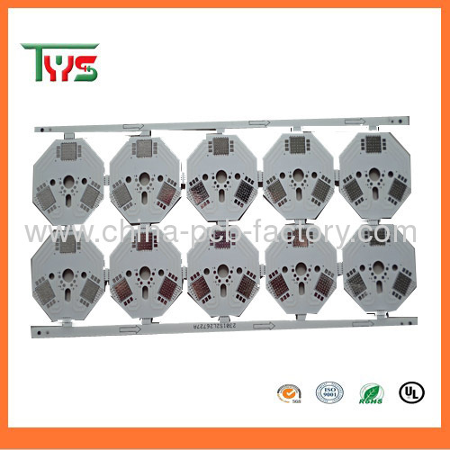
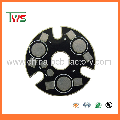
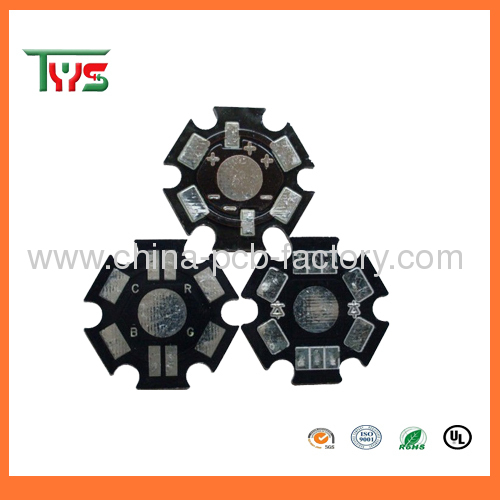
LED downlight circuit board
0.1~1.0 USD
| Min. Order: | 5 Piece/Pieces |
|---|---|
| Payment Terms: | Paypal, T/T, WU |
| Supply Ability: | 120000 Square Meter /Month |
| Place of Origin: | Guangdong |
Company Profile
| Location: | Shenzhen, Guangdong, China (Mainland) |
|---|---|
| Business Type: | Manufacturer |
| Main Products: | PCB |
Product Detail
| Model No.: | TWS-C02F |
|---|---|
| Means of Transport: | Ocean, Land |
| Brand Name: | TWS |
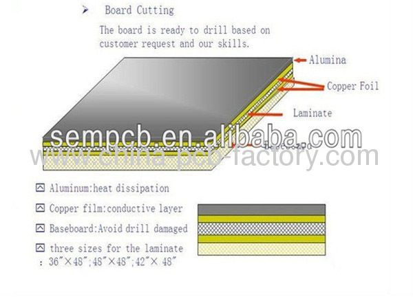
| Base Material: | Aluminum |
| Copper Thickness: | 1oz |
| Board Thickness: | 1.6mm |
| Min. Hole Size: | 0.15mm |
| Min. Line Width: | 0.2mm |
| Min. Line Spacing: | 0.2mm |
| Surface Finishing: | LF HASL |
| Layer: | 1-28 Layer |
| Solder Mask: | green/red/blue/white/yellow |
| MAX.Board Size: | 9200*900mm |
| Certification: | UL/SGS/ROHS |
| Controlled impedance: | ±5% |
| Warp&Twist: | 0.7% |
| Rang of finish boards thickness: | 0.21~7.0mm |
| Impedance control: | ±10% |
| OEM/ODM: | One-stop service |
| PCB standard: | IPC-A-610D |
| Production Capacity: | 120000 Square Meter /Month |
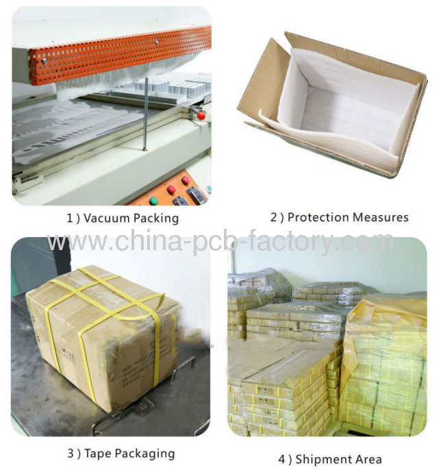
| Packing: | vacuum packaging and carton box |
| Delivery Date: | 5-15 working days after your payments |
Product Description
LED downlight circuit board
Capacity of pcb
4.Service
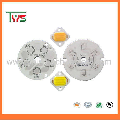
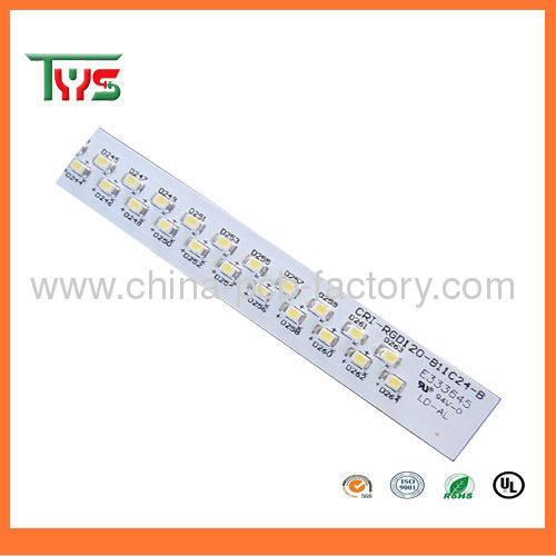
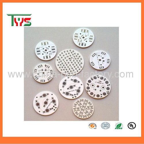
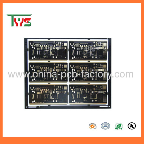
1.FR4,6 layer,HASL,1.6MM,impedance controlled rigid flex pcb board ,
2.100% E-tested
3. UL approved on requirements of materials, solder mask, and conductor widths and spacing. All materials purchased and used in manufacturing have a flammability rating to 94V-O.
4.Track your oder on time
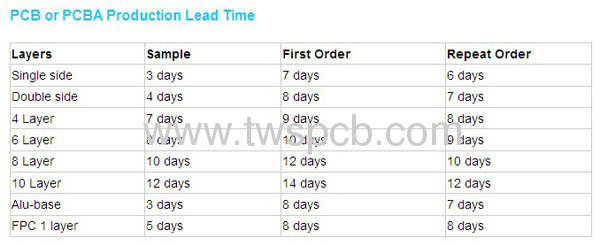
5.Lead time is manufacturing+shipping time
Technical requirement:1) Professional Surface-mounting and Through-hole soldering Technology
2) Various sizes like 1206,0805,0603 components SMT technology
3) ICT(In Circuit Test),FCT(Functional Circuit Test) technology.
4) PCB Assembly With UL,CE,FCC,Rohs Approval
5) Nitrogen gas reflow soldering technology for SMT.
6) High Standard SMT&Solder Assembly Line
7) High density interconnected board placement technology capacity.
Quote requirement:
- Gerber file of the bare PCB board
- BOM (Bill of material) for assembly
- To short the lead time, please kindly advise us if there is any acceptable components substitution.
- Testing Guide & Test Fixtures if necessary
- Programming files & Programming tool if necessary
- Schematic if necessary
OEM/ODM/EMS Services for PCBA:
- PCBA, PCB assembly: SMT & PTH & BGA
- PCBA and enclosure design
- Components sourcing and purchasing
- Quick prototyping
- Plastic injection molding
- Metal sheet stamping
- Final assembly
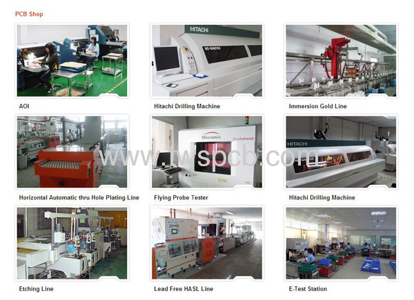
- Test: AOI, In-Circuit Test (ICT), Functional Test (FCT)
- Custom clearance for material importing and product exporting
Orientronic PCB assembly Equipment:
- SMT Machine: SIEMENS SIPLACE D1/D2 / SIEMENS SIPLACE S20/F4
- Reflow Oven: FolunGwin FL-RX860
- Wave Soldering Machine: FolunGwin ADS300
- Automated Optical Inspection (AOI): Aleader ALD-H-350B
- Fully Automatic SMT Stencil Printer: FolunGwin Win-5
Capacity of pcb
NO | ITEM | Technical Data |
1 | Layer | 2-20 Layers |
2 | Board material | FR4,FR4 Halogen free,TEFLON Rogers,Getek High-TG(TG>170),Aluminium base |
3 | Max.Board Size0 | 457*660mm |
4 | Min.Board Thickness | 2 layers 0.2mm |
4 layers 0.4mm | ||
6 layers 0.8mm | ||
8 layers 1.0mm | ||
10 layers 1.2mm | ||
5 | Max.Board Thickness | 8.0mm |
6 | Min.Line Width | 0.05mm |
7 | Min.Line Space | 0.05mm |
8 | Min.Hole Size0 | Electroplating Via 0.15mm |
Micro via 0.075mm | ||
9 | PTH Wall Thickness) | 20-25um |
10 | Max.finish copper thickness0 | 8OZ |
11 | PTH Dia.Tolerance | ±0.05mm |
12 | NPTH Dia.Tolerance | ±0.025mm |
13 | Hole Position Deviation | ±0.05mm |
14 | Outline Tolerance | ±0.1mm |
15 | Min.S/M Pitch | 0.08mm |
16 | Insulation Resistance | 3x10Sec, 288°C |
17 | Warp and Twist | ≤0.7% |
18 | Electric Strength | >1.3KV/mm |
19 | Peel Strength | ≥1.4N/mm |
20 | Solder Mask Abrasion | ≥6H |
21 | Flammability | 94V0 |
22 | Impedance Control | ±5% |
PCB Superiority
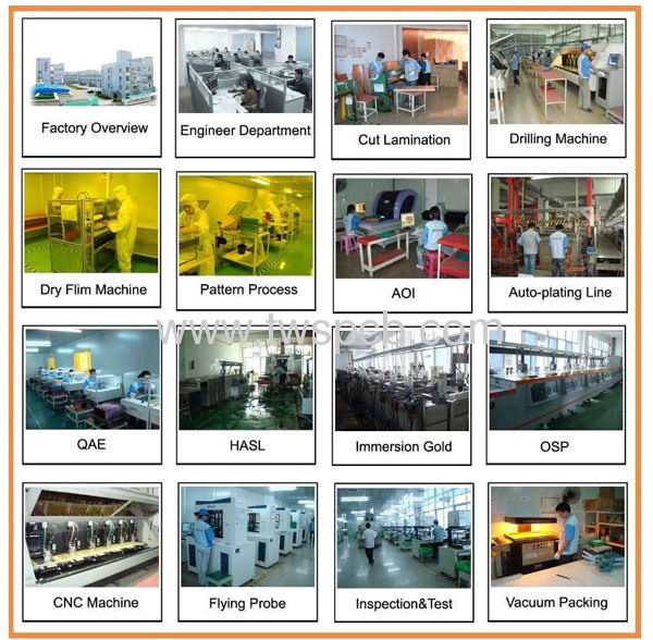
1.High efficiency&Experience
1.High efficiency&Experience
We can provide one stop service.Established in 1998, with many years hard-working and constant innovation,we have
grown up into a professional PCB&PCBA manufacturer. We have our own independent research and development
department and sophisticated quality control system.
--------------------------------------------------------------------------------
2.Quality
Our product are manufactured according to the UL/Rohs standards to insure quality assemblies from start to finish. Whether
Our product are manufactured according to the UL/Rohs standards to insure quality assemblies from start to finish. Whether
it's a simple custom or not.Product or a complex turnkey production run, We will adhere to the highest quality standards.
--------------------------------------------------------------------------------
3.Protecting your interests
Protecting your Intellectual Property is job one! Our staff of trained professionals are all working under a strict confidentiality
Protecting your Intellectual Property is job one! Our staff of trained professionals are all working under a strict confidentiality
contract and treat your important documentation as they would their own.
--------------------------------------------------------------------------------
4.Service
We can provide 24hours service for you. We pride ourselves on our ability to custom tailor programs around our customers'
needs.We take time to listen to your unique business needs and then set out to surpass them.


LED DOWNLIGHT CIRCUIT BOARD


