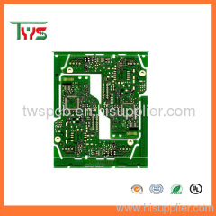
FR4 1.2mm double sided pcb with lead free HASL
0.02~0.3 USD
| Min. Order: | 10 Piece/Pieces |
|---|---|
| Trade Term: | FOB |
| Payment Terms: | L/C, T/T, WU |
| Supply Ability: | 10000 square meter |
| Place of Origin: | Guangdong |
Company Profile
| Location: | Shenzhen, Guangdong, China (Mainland) |
|---|---|
| Business Type: | Manufacturer |
| Main Products: | PCB |
Product Detail
| Model No.: | tws-2013070108 |
|---|---|
| Means of Transport: | Ocean, Air, Land |
| Brand Name: | TWS |
| Base Material: | FR4 |
| Copper Thickness: | 1OZ |
| Board Thickness: | 1.2mm |
| Min. Hole Size: | 0.35mm |
| Min. Line Width: | 0.25mm |
| Min. Line Spacing: | 0.25mm |
| Surface Finishing: | HASL |
| Surface Finishing: | HASL,ENIG,OSP,immersion gold/silver/tin,gold plating,Gold finger |
| color: | all colours |
| contouring: | milling and V-cut |
| Shape tolerance: | +/-0.13 |
| Tolerance of finished panel thickness: | +/-10% |
| Standard: | IPC-A-610D |
| Certification: | UL,ISO |
| legend colour: | white |
| Name: | FR4 1.2mm double sided pcb with lead free HASL |
| Production Capacity: | 10000 square meter |
| Packing: | vacuum plastic and carton, suitable for any means of transport; |
| Delivery Date: | 5-7 working days |
Product Description
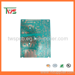
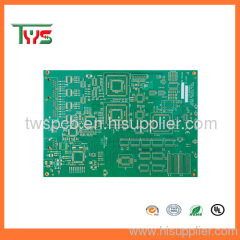
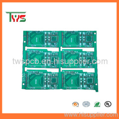
FR4 1.2mm double sided pcb with lead free HASL

2.Honesty credibility inchina's top.
3.Competest price but high quality.
4. One-stopservice.
5.Delivery ontime.
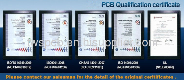
What products we can do for you:
1. FR4 pcb(1-26L)
2. Aluminumpcb(1-2L)
3. CEM-1,CEM-3,94V-0pcb(1-2L)
4. High TGpcb(TG170,TG150)
5. Flex pcb(1-6L)
6. Rigid-flexpcb(1-6L)
1> PCB ProcessingDetails:
2>PCB Package &Delivery:
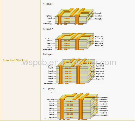
Our packingdetails:

Delivery time:
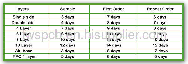
What's superiority for us?
Quality


------Tianweisheng Electronic Co.,Ltd
Welcometo.......Tian Wei Sheng
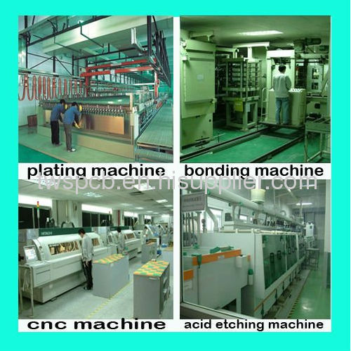
1.Advanced production linesand professional staff.
2.Honesty credibility inchina's top.
3.Competest price but high quality.
4. One-stopservice.
5.Delivery ontime.

What products we can do for you:
1. FR4 pcb(1-26L)
2. Aluminumpcb(1-2L)
3. CEM-1,CEM-3,94V-0pcb(1-2L)
4. High TGpcb(TG170,TG150)
5. Flex pcb(1-6L)
6. Rigid-flexpcb(1-6L)
1> PCB ProcessingDetails:
Place ofOrigin shenzhen China(mainland) | Brandname:TWS-PCB | ModelNumber:4layer |
Basematerial:FR-4 | Copperthickness:1oz | Boardthickness:1.6mm |
Min.Holesize:0.2mm | Min.linewidth:4mil | Min. LineSpace:4mil |
SurfaceFinishing:immersion gold | Soldermask:green | Legend :White |
Test:E-testing |
.
2>PCB Package &Delivery:
Packdetails: | Vacuumpacking,export carton |
Deliverytime: | 5-7days |
Productivity | ||
Item | Technicalstandards | |
Rise | 1-26layer | |
Material | CEM-1,CEM-3,FR-4,FR4TG170,TG180 ,HALOGEN FREE | |
Lamellar | 0.2mm-3.20m(8mil-126mil) | |
Minimumthickness | 0.1mm(4mil) | |
Thick copper | 0.5-6 OZ | |
Min line w / s | 0.075mm(3mil) | |
Min Hole Side | 0.20mm(8mil) | |
Min apertureChong | 0.9mm(35mil) | |
Tolerance | Hole drillingbit | ±0.075mm(3mil) |
Linewidth | ±0.05mm(2mil)Orwidth of ±20% | |
Aperture | PTH±0.075mm(3mil) | |
NPTH±0.05mm(2mil) | ||
Shapetolerance | MillingMachine±0.15mm(6mil) | |
Punch±0.10mm(4mil) | ||
Warp | 0.70%-1.5% | |
Pad surfacetreatment | Nickel/Gold Finger Plating/FlashGold/Entek/LEAD Free Hal | |
InsulationResistance | 10k-20MΩ | |
Conductionresistance | <50Ω | |
Test voltage | 300v | |
V Engraved | Panle size | 110*100mm(min.)660*600mm(max.) |
Thickness | 0.6mm(24mil)min. | |
Retention ofthe thickness | 0.3mm(12mil)min. | |
Tolerance | ±0.1mm(4mil) | |
Width | 0.50mm(20mil)max. | |
Trough to aline | 0.5mm(20mil)min | |
Trough | Slot sizetlo.≥2WTolerance | PTHL:±0.15mm(6mil) |
W:±0.1mm(4mil) | ||
NPTH:±0.125mm(5mil) | ||
W:±0.1mm(4mil) | ||
To circularfrom the hole | PTH Hole:0.13mm(5mil) | NPTH Hole:0.18(7mil) |
MLB | Circulardeviation | 0.075mm(3mil) |
Deviationbetween layers | 4 layers:0.15mm(6mil)max | |
6 layers:0.025mm(10mil)max. | ||
Aperture tothe smallest distance from theinner circle | 0.25mm(10mil) | |
To circularfromthe hole | 0.25mm(10mil) | |
ThicknessTolerance | 6 layers:±0.15mm(6mil) | |
6 layers:±0.15mm(6mil) | ||
CharacteristicImpedance | 60Ω±10% | |

Our packingdetails:

Delivery time:

What's superiority for us?
Quality
Our UL/Rohsstandards insure the production quality from PCB farbication to delivery, eachlink is
we highly valued, all what we do is to satisfy our customer ToBe The Best!
--------------------------------------------------------------------------------
Experience
Since built in 1998,ourmanagement teamwork has over 14years of combined industryknowledge,
Experience
Since built in 1998,ourmanagement teamwork has over 14years of combined industryknowledge,
The Engineers, QCs and OP have strong qualitysenses.
--------------------------------------------------------------------------------
Confidentiality
--------------------------------------------------------------------------------
Confidentiality
It include the Intellectual Property and the companyinformation of our customers, also it is every stuff's
responsibility to protect the information ofcustomers.
--------------------------------------------------------------------------------
Flexibility
From the PCB circuitboard producing to packing and shiping, every produce details runs according tocustomer's
Flexibility
From the PCB circuitboard producing to packing and shiping, every produce details runs according tocustomer's
request.

PurchaseTips:
A.For PCB order,please provide Gerber file or *.pcb file. Any details are also welcomed if noGerber file.
B.Large PCB quantityorder, quotation will be based on SQM.
C.For PCBA order,please provide the Gerber file, *.pcb file and BOM List.
D.Reverse engineeringand PCB clone service can be supplied with your printed circuit boardsupplied.
E.Any questions,welcome to contact our sales person Ann by sending inquiry. Your satisfactionis our pleasure.

We have a profesional PCB and PCBA manufacturer in China, we can supply PCBDesign,PCB Layout,PCBFabrication, Pls contact us for more informations if you have anyinterests in our products.
THANKS FOR YOUR SUPPORT !

THANKS FOR YOUR SUPPORT !

