
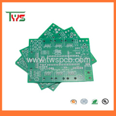
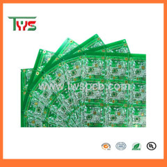
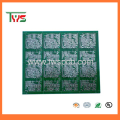
High class multilayer printed circuit board manufacturing
0.1~1.0 USD
| Min. Order: | 5 Piece/Pieces |
|---|---|
| Payment Terms: | Paypal, T/T, WU |
| Supply Ability: | 30000 Square Meter /Month |
| Place of Origin: | Guangdong |
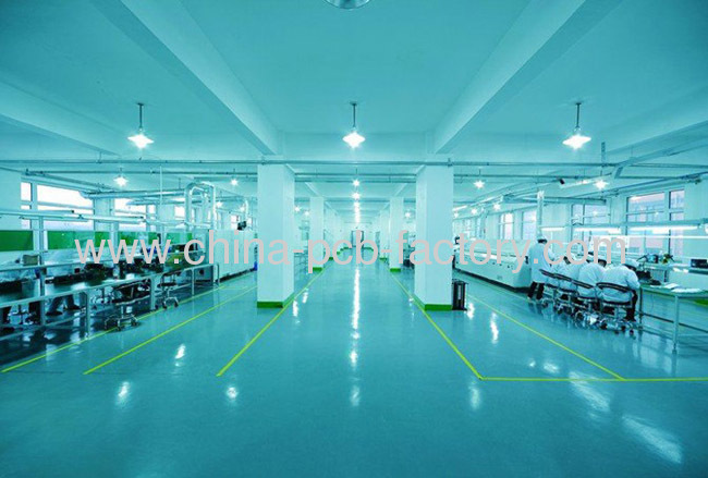
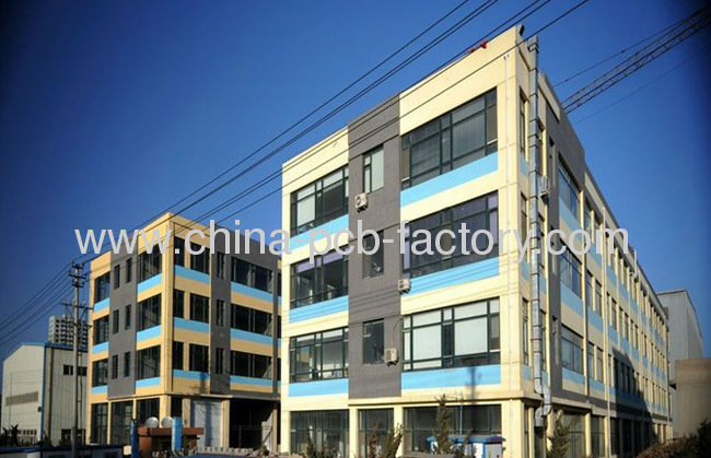
Company Profile
| Location: | Shenzhen, Guangdong, China (Mainland) |
|---|---|
| Business Type: | Manufacturer |
| Main Products: | PCB |
Product Detail
| Model No.: | TWS-A01K |
|---|---|
| Means of Transport: | Ocean, Air, Land |
| Brand Name: | TWS |
| Base Material: | FR-1,FR-2,FR-4,CEM-1,CEM-3,Hight TG,FR4 Halogen Free,Aluminum material |
| Copper Thickness: | 0.5-4.0oz |
| Board Thickness: | 0.2mm-7mm |
| Min. Hole Diameter: | 0.25mm |
| Min. Line Width: | 0.075mm(3mil) |
| Min. Line Spacing: | 0.075mm(3mil) |
| Surface Finishing: | HALS/HALS lead free,Chemical tin,Chemical Gold,Immersion gold Inmersion Silver/Gold,Osp,Gold Plating |
| Layer: | 1-28 Layer |
| Solder Mask: | green/red/blue/white/yellow |
| MAX.Board Size: | 9200*900mm |
| Certification: | UL/SGS/ROHS |
| Controlled impedance: | ±5% |
| Warp&Twist: | 0.7% |
| Rang of finish boards thickness: | 0.21~7.0mm |
| Impedance control: | ±10% |
| OEM/ODM: | One-stop service |
| PCB standard: | IPC-A-610D |
| Production Capacity: | 30000 Square Meter /Month |
| Packing: | vacuum packaging and carton box |
| Delivery Date: | 5-15 working days after your payments |
Product Description
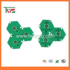
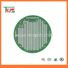
printed circuit board manufacturing
PCB fabrication/design & development stages:
PCB Superiority
1.High efficiency&Experience
4.Service

1) layer: 1-28 PCB
2) PCBBoard finished thickness: 0.2mm-7.0mm
3) Material: FR-4, CEM-3, High TG, FR4 Halogen Free, Rogers.
4) Max. Finished board size: 580mm*900mm
5) Min hole size: 4mil(0.1mm)
6) Min trace width/space: 3.5mil/3.5mil
7) Surface finishing/treatment: HASL/Lead free HASL, Immersion Gold, Gold plating,Immersion silver, immersion Tin, OSP.
8) Copper thickness: 0.5oz to 6oz.
9) Copper thickness in hole: >18um
10) Inner packing: Vacuum packing/plastic bag
11) Outline tolerance:+/-0.13mm
Hole size tolerance: PTH+/-0.076mm NPTH:+/-0.05mm.
12) Quality ensure: UL approval, TS16949:2002
13) Special requirements: Buried and Blind vias, impedance control, via plug, BGA soldering, Gold finger.
14) Profiling: punching, Routing, V-cut, Beveling.
15) Provides OEM services to all sorts of printed circuit board assembly as well as Electronic encased products.
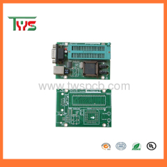
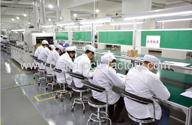
PCB/PCBAssembly/PCBA OEM suppliers
1. We have the most advanced SMT machine Mydata which is fully automatic. It can distinguish component's direction automatically during soldering, finding correct components value if the operator put the component at a wrong place.
2. Our solder paste printer is also automatically which is more precise and symmetrical, all of them are imported from Japan. (KOKI)
3. We have wave soldering machine to do through-hole soldering, supporting large-scale need.
4. We do 100% AOI testing after surface mount, which can check out components'missing, wrong direction, solder insufficient, ect.
5. Our management system is TS16949: 2002, since we provide OEM service for auto parts in car stalk ,like Honda, BMW ect.
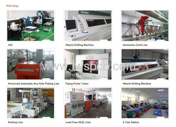
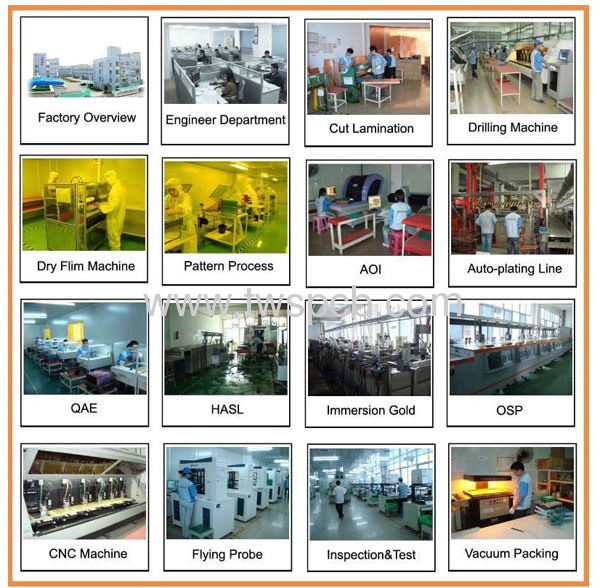
Equipment
Equipment
SMT (Surface mount technology)
Fourcomplete SMT lines comprised of the following machines:
- Quantity 4– MYDATA MY15E
- MYDATAMY12
- Quantity 2– UNIVERSAL-4796 HSP
- UNIVERSAL-4797LHSP
- Quantity 3EKRA- X4
- EKRA-X5
- TRITON IVMIL SMT (aqueous cleaner)
Throughhole
- UniversalTH- Radial
- UniversalTH- VCD-Sequencer
- UniversalTH- Dip
Quality Assurance& Quality Control
- VantageS22™ - Post-Reflow AOI System
- Marantz -NSPECFV18
PCB fabrication/design & development stages:
1. Requirements & Specifications
2. Preliminary Design Review (PDR)
3. Critical PCB Design Review (CDR)
4. Alpha PCB Prototype Phase
5. PCB design service: Beta Prototype Phase
6. Production Readiness
Capacity of pcbItem | Manufacture Capability | |
Material | FR-4 / Hi Tg FR-4 / Lead free Materials (RoHS Compliant),Aluminium, Metal based | |
Layer No. | 1-16 | |
Finished Board thickness | 0.20 mm-6.0mm'(8 mil-150 mil) | |
Board Thickness Tolerance | ±10% | |
Cooper thickness | 0.5 OZ-6OZ (18 um-210 um) | |
Copper Plating Hole | 18-40 um | |
Impedance Control | ±10% | |
Warp&Twist | 0.70% | |
Peelable | 0.012"(0.3mm)-0.02'(0.5mm) | |
Images | ||
Min Trace Width (a) | 0.075mm (3mil) | |
Min Space Width (b) | 0.1mm (4 mil) | |
Min Annular Ring | 0.1mm (4 mil) | |
SMD Pitch (a) | 0.2 mm(8 mil) | |
BGA Pitch (b) | 0.2 mm (8 mil) | |
0.05mm | ||
Solder Mask | ||
Min Solder Mask Dam (a) | 0.0635 mm (2.5mil) | |
Soldermask Clearance (b) | 0.1mm (4 mil) | |
Min SMT Pad spacing (c) | 0.1mm (4 mil) | |
Solder Mask Thickness | 0.0007"(0.018mm) | |
Holes | ||
Min Hole size (CNC) | 0.2 mm (8 mil) | |
Min Punch Hole Size | 0.9 mm (35 mil) | |
Hole Size Tol (+/-) | PTH:±0.075mm;NPTH: ±0.05mm | |
Hole Position Tol | ±0.075mm | |
Plating | ||
HASL | 2.5um | |
Lead free HASL | 2.5um | |
Immersion Gold | Nickel3-7umAu:1-5u'' | |
OSP | 0.2-0.5um | |
Outline | ||
Panel Outline Tol (+/-) | CNC: ±0.125mm, Punching: ±0.15mm | |
Beveling | 30°45° | |
Gold Finger angle | 15° 30° 45° 60° | |
Certificate | ROHS,ISO9001:2008,SGS,UL certificate | |
PCB Superiority
1.High efficiency&Experience
We can provide one stop service.Established in 1998, with many years hard-working and constant innovation,we have
grown up into a professional PCB&PCBA manufacturer. We have our own independent research and development
department and sophisticated quality control system.
--------------------------------------------------------------------------------
2.Quality
Our product are manufactured according to the UL/Rohs standards to insure quality assemblies from start to finish. Whether
Our product are manufactured according to the UL/Rohs standards to insure quality assemblies from start to finish. Whether
it's a simple custom or not.Product or a complex turnkey production run, We will adhere to the highest quality standards.
--------------------------------------------------------------------------------
3.Protecting your interests
Protecting your Intellectual Property is job one! Our staff of trained professionals are all working under a strict confidentiality
Protecting your Intellectual Property is job one! Our staff of trained professionals are all working under a strict confidentiality
contract and treat your important documentation as they would their own.
--------------------------------------------------------------------------------
4.Service
We can provide 24hours service for you. We pride ourselves on our ability to custom tailor programs around our customers'
needs.We take time to listen to your unique business needs and then set out to surpass them.
If you are interested,pls sent me your Gerber files and PCB Specifications(such as copper thickness:18um or 35um?,board thickness:0.8mm or 1.6mm?,surface treatment:lead-free HASL or immersion gold?),if it's the PCBA,pls sent me the BOM list(including all components details),then we will quote for your at first time,we always try our best,
you will find that we are the right PCB supplier you want.
PRINTED CIRCUIT BOARD MANUFACTURER