
Leading Shenzhen factory supplier for PCBA EMS
57.0~200.0 USD
| Min. Order: | 1 Square Meter |
|---|---|
| Trade Term: | FOB |
| Payment Terms: | L/C, D/P, D/A, T/T, WU |
| Supply Ability: | 1000square meter/per day |
| Place of Origin: | Guangdong |
Company Profile
| Location: | Shenzhen, Guangdong, China (Mainland) |
|---|---|
| Business Type: | Manufacturer |
| Main Products: | PCB |
Product Detail
| Model No.: | 795-is |
|---|---|
| Means of Transport: | Ocean, Air, Land |
| Max pane size: | 34"*25" |
| Independence tolerance: | +/-18% |
| Aspecr Ratio: | 10:7 |
| Layer count: | 1-24 |
| Solder mask abrasion: | ≥10H |
| Gold finger: | Ni: 80~250u", Au: 1~5u" |
| Warp and twist: | ≤0.55% |
| Via plug: | Max via size: 24mil (0.6mm) |
| Peel Strength: | 1.4N/mm |
| Certification: | UL/SGS/ROHS |
| Production Capacity: | 1000square meter/per day |
| Packing: | Inner vacuum and plastic package,outer carton box package |
| Delivery Date: | 3~10days |
Product Description
Specifications
Leading Shenzhen factory supplier for PCBA EMS
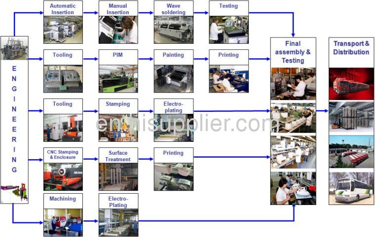
1.onestop service
2.AOI checking
3.X-ray checking
4.reliable factory
1.onestop service
2.AOI checking
3.X-ray checking
4.reliable factory
Leading Shenzhen factory supplier for PCBA EMS__________________________________________________________________________________________________
PCBManufacture Capability
Item | Capability | |
1.Base Material | FR-4 / High TG FR-4 / Lead free Materials (ROHS Compliant) / Halogen Freematerial /CEM-3/CEM-1/ /PTFE/ROGERS/ARLON/TACONIC | |
2.Layers | 1-28 | |
3.Finised inner/outer copper thickness | 1-6OZ | |
4.Finished board thickness | 0.2-7.0mm | |
Tolerance | Board thickness≤1.0mm: +/-0.1mm 1<Board thickness≤2.0mm: +/-10% Board thickness>2.0mm: +/-8% | |
5.Max panel size | ≤2sidesPCB: 600*1500mm Multilayer PCB: 500*1200mm | |
6.Min conductor line width/spacing | Inner layers: ≥3/3mil Outer layers: ≥3.5/3.5mil | |
7.Min hole size | Mechanical hole: 0.15mm Laser hole: 0.1mm | |
Drilling precision: first drilling | First drilling: 1mil Second drilling: 4mil | |
8.Warpage | Board thickness≤0.79mm: β≤1.0% 0.80≤Board thickness≤2.4mm: β≤0.7% Board thickness≥2.5mm: β≤0.5% | |
9.Controlled Impedance | +/-5% | |
10. Aspect Ratio | 15:1 | |
11.Min welding ring | 4mil | |
12.Min solder mask bridge | ≥0.08mm | |
13.Plugging vias capability | 0.2-0.8mm | |
14. Hole tolerance | PTH: +/-3mil NPTH: +/-2mil | |
15.Outline profile | Rout/ V-cut/ Bridge/ Stamp hole | |
16.Surface treatment | OSP: 0.5-0.5um HASL: 2-40um Lead free HASL: 2-40um ENIG: Au 1-10U'' ENEPIG: PB 2-5U''/ Au 1-8U'' Immersion Tin:0.8-1.2um Immersion silver: 0.1-1.2um Peelable blue mask Carbon ink Gold plating: Au 1-150U'' | |
17. E-testing pass percent | 97% pass for the first time,+/-2%(tolerance) | |
FQC-Physical Lab: Reliability tests | ||
18.Certificate | ROHSUL:E327776ISO9001:2008IPCSGS | |
Our equipments | ||
1.Drilling workshop | 4 drilling bits of drilling machine: 4 sets 2 drilling bits of drilling machine: 2 sets | |
2. photo plotting workshop | Israel "ORBOTECH" Photo Plotters | |
3.AOI | AOI machine | |
4.IPQC | "OXFORD" CMI 700 Copper Thickness Tester | |
5.Impedance test | USA "Tektronix" DSA 8200 Impedance Tester | |
6.Outline workshop | CNC routing machine: 7 sets angle-cutting machine V-cut machine | |
7.Testing Workshop | Surpass X-600: 2sets WTD FT-2808: 5sets WTD HV300: 1set | |
8.X-ray | X-ray machine | |
Acceptable file format | ||
GERBER file, PROTEL series, PADS series, POWER PCB series, AutoCADseries. | ||
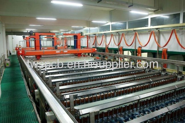
Advanced ProductionEquipment
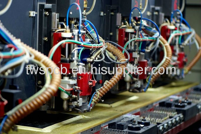


Product HighQuality Perfect
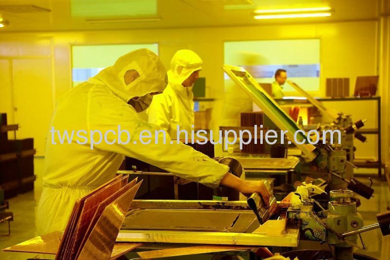

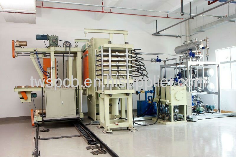
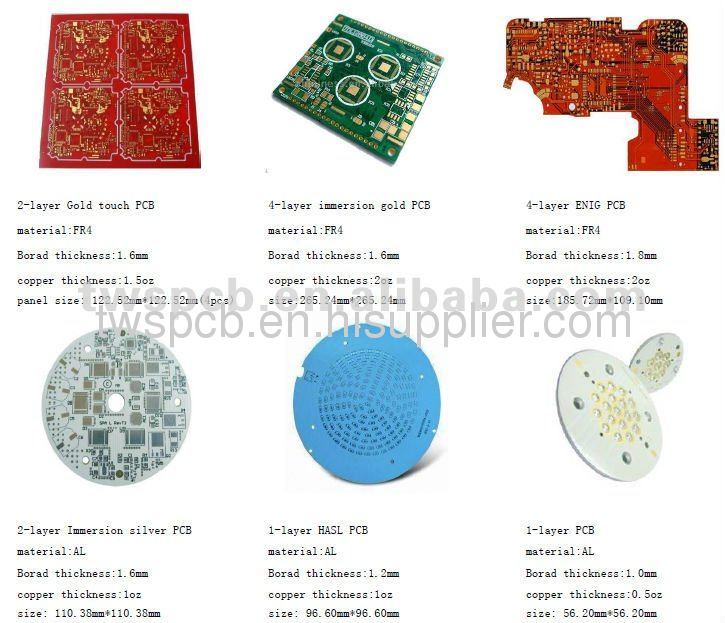
Meet your need is ourgreatest pursuit .If you are looking for a pcb board manufacturerinchina,Pleasegive us your files ofpcb for a quote (Gerberfiles and specification),I will reply email in 3hours. Youalso cancontact usby .
1.Advanced production lines andprofessional staff.
2.Honesty credibility in china'stop.
3.Competest price but highquality.
4. One-stopservice.
5.Delivery ontime.
