
Shenzhen PCB Manufacturer Electronics Manufacturing Services
57.0~200.0 USD
| Min. Order: | 1 Square Meter |
|---|---|
| Trade Term: | FOB |
| Payment Terms: | L/C, D/P, D/A, T/T, WU |
| Supply Ability: | 1000square meter/per day |
| Place of Origin: | Guangdong |
Company Profile
| Location: | Shenzhen, Guangdong, China (Mainland) |
|---|---|
| Business Type: | Manufacturer |
| Main Products: | PCB |
Product Detail
| Model No.: | TR9530 |
|---|---|
| Means of Transport: | Ocean, Air, Land |
| Max pane size: | 34"*20" |
| Independence tolerance: | +/-16% |
| Aspecr Ratio: | 10:1 |
| Layer count: | 1-20 |
| Solder mask abrasion: | ≥9H |
| Gold finger: | Ni: 80~250u", Au: 1~5u" |
| Warp and twist: | ≤0.55% |
| Via plug: | Max via size: 24mil (0.6mm) |
| Peel Strength: | 1.4N/mm |
| Certification: | UL/SGS/ROHS |
| Production Capacity: | 1000square meter/per day |
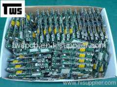
| Packing: | Inner vacuum and plastic package,outer carton box package |
| Delivery Date: | 3~10days |
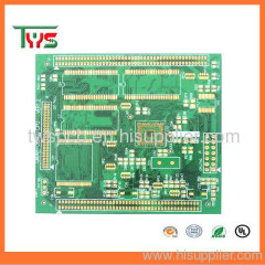
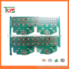
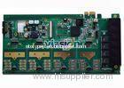
Product Description
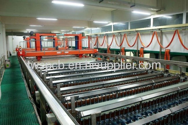
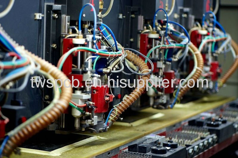
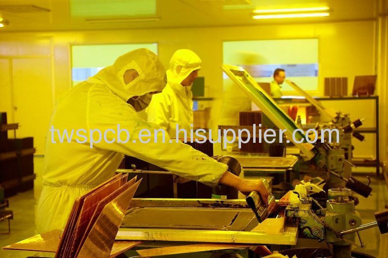
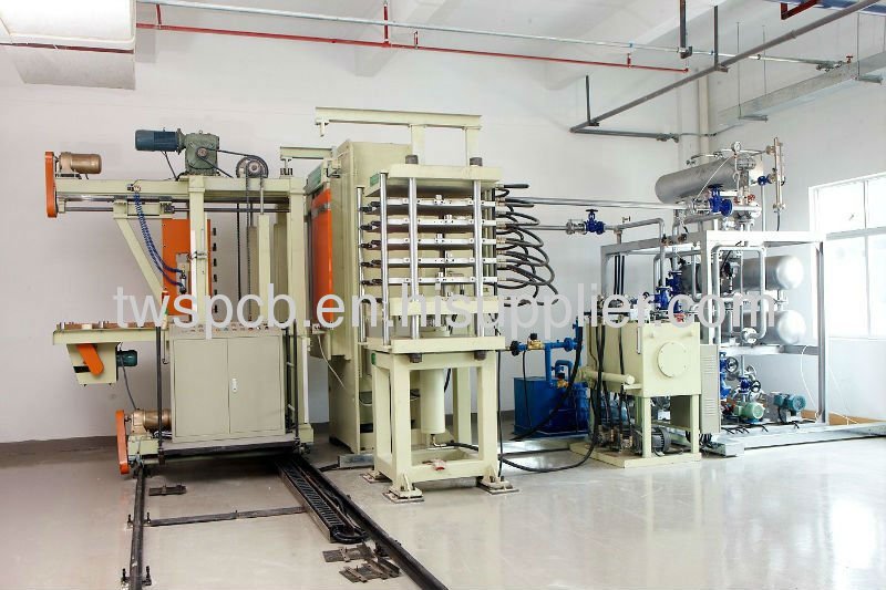
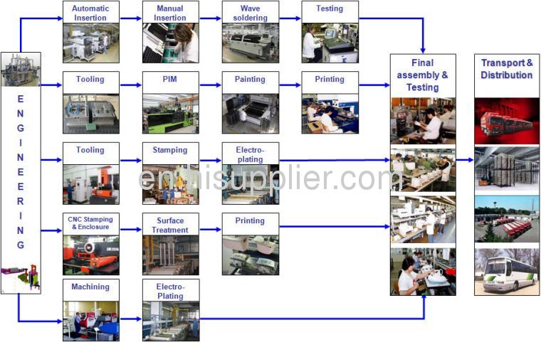
Advanced ProductionEquipment
Product HighQuality Perfect
Meet your need is ourgreatest pursuit .If you are looking for a pcb board manufacturerinchina,Pleasegive us your files ofpcb for a quote (Gerberfiles and specification),I will reply email in 3hours. Youalso cancontact usby .
1.Advanced production lines andprofessional staff.
2.Honesty credibility in china'stop.
3.Competest price but highquality.
4. One-stopservice.
5.Delivery ontime.
Specifications
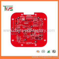
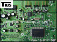
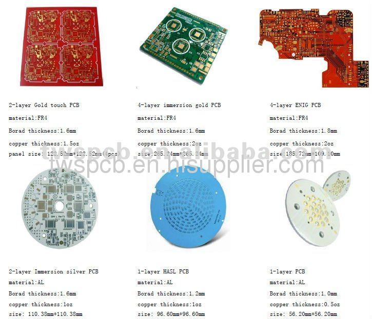
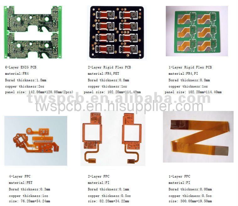
4-layer Printed Circuit Board / 4-layer pcb
1.20 yearsexperance
2.Provide OEM PCB
3.UL; ISO accept
4.Vacuum package
1.20 yearsexperance
2.Provide OEM PCB
3.UL; ISO accept
4.Vacuum package
Description of our4-layer Printed Circuit Board / 4-layer pcb :
1) Min.Trace width: 0.20mm
2) Min. Space between trace: 0.20mm
3) Min. Holesize: 0.5mm
4) Thickness tolerance:
A) Single sided: 0.005"
B) Doublesided: 0.010"
5) Base materials: Polyimide and polyester
6) Conductor(copper thickness): 0.5oz., 1oz. And 2oz. (RA and ED copper)
7) Cover-layer:Polyimide and polyester (solder mask printing is available)
8) Adhesivematerial: Epoxy, acrylic and polyester
9) Stiffener materials: FR-4, mylarand polyimide
10) Surface finishes: Flash gold plating, selective goldplating and solder plating Package:Vacuum package
| NO | Item | Craft Capacity |
| 1 | Layer | 1-30 Layers |
| 2 | Base Material for PCB | FR4, CEM-1, TACONIC, Aluminium, High Tg Material, High Frequence ROGERS ,TEFLON, ARLON, Halogen-free Material |
| 3 | Rang of finish baords Thickness | 0.21-7.0mm |
| 4 | Max size of finish board | 900MM*900MM |
| 5 | Minimum Linewidth | 3mil (0.075mm) |
| 6 | Minimum Line space | 3mil (0.075mm) |
| 7 | Min space between pad to pad | 3mil (0.075mm) |
| 8 | Minimum hole diameter | 0.10 mm |
| 9 | Min bonding pad diameter | 10mil |
| 10 | Max proportion of drilling hole and board thickness | 1:12.5 |
| 11 | Minimum linewidth of Idents | 4mil |
| 12 | Min Height of Idents | 25mil |
| 13 | Finishing Treatment | HASL (Tin-Lead Free), ENIG(Immersion Gold), Immersion Silver , Gold Plating (Flash Gold), OSP, etc. |
| 14 | Soldermask | Green, White, Red, Yellow, Black, Blue, transparent photosensitive soldermask, Strippable soldermask. |
| 15 | Minimun thickness of soldermask | 10um |
| 16 | Color of silk-screen | White, Black, Yellow ect. |
| 17 | E-Testing | 100% E-Testing (High Voltage Testing); Flying Probe Testing |
| 18 | Other test | ImpedanceTesting,Resistance Testing, Microsection etc., |
| 19 | Date file format | GERBER FILE and DRILLING FILE, PROTEL SERIES, PADS2000 SERIES, Powerpcb SERIES, ODB++ |
| 20 | Special technological requirement | Blind & Buried Vias and High Thickness copper |
| 21 | Thickness of Copper | 0.5-14oz (18-490um) |