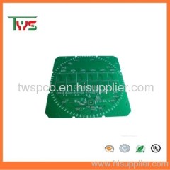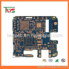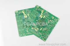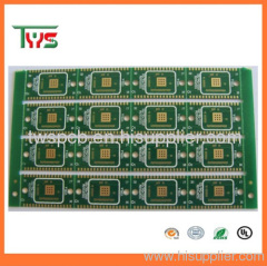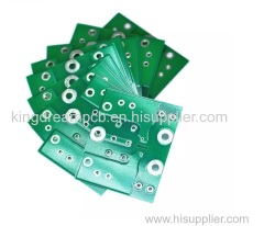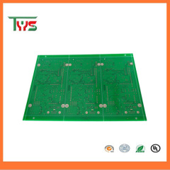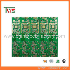
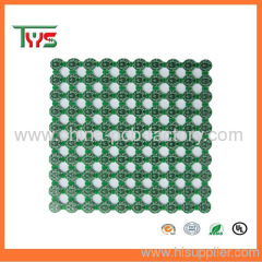
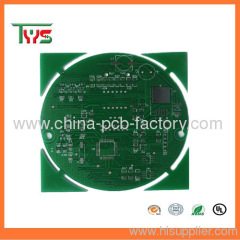
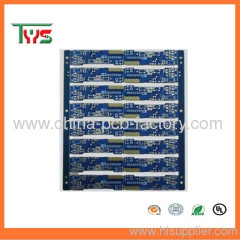
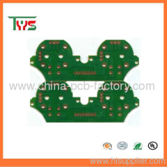
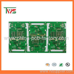
High quality 4 layer pcb manufacturer
0.1~0.5 USD
| Min. Order: | 10 Piece/Pieces |
|---|---|
| Trade Term: | FOB |
| Payment Terms: | Paypal, T/T, WU |
| Supply Ability: | 300000 Square meter/Month |
| Place of Origin: | Guangdong |
Company Profile
| Location: | Shenzhen, Guangdong, China (Mainland) |
|---|---|
| Business Type: | Manufacturer |
| Main Products: | PCB |
Product Detail
| Model No.: | tws-h01 |
|---|---|
| Means of Transport: | Ocean, Air, Land |
| Number of Layers: | 4-Layer |
| Brand Name: | tws |
| Base Material: | fr4 |
| Copper Thickness: | 1oz |
| Board Thickness: | 1.4mm |
| Min. Hole Size: | 0.15mm |
| Min. Line Width: | 0.2mm |
| Min. Line Spacing: | 0.2mm |
| Soldermask color: | Green/Blue/Black/Red/White etc |
| Silkscreen color: | White/Black/Yellow etc |
| Surface finishing: | HASL/OSP/ENIG etc |
| OEM/ODM: | One-stop service |
| PCB standard: | IPC-A-610D |
| Maz size of finish board: | 900*900mm |
| E-testing: | 100% E-testing, Flying probe testing |
| Layer number: | 1~28L |
| Certification: | UL/RoHS/SGS |
| Impedance control: | ±5% |
| Production Capacity: | 300000 Square meter/Month |
| Packing: | vacuum package+carton box |
| Delivery Date: | 5 days for pcb sample, 15 days for mass pcb order. |
Product Description
4 layer pcb manufacturer
4.Service


1. PCB board file with parts list provided by customers;
2. PCB board made, circuit board parts purchased by us;
3. PCB board with parts assembled;
4. Electronic testing circuit board or PCBA;
5. Fast delivery, anti-static package;
6.RoHS Directive-compliant, lead-free;
7. One stop service for PCB design, PCB layout, PCB manufacture, components purchasing, PCB assembly, test, packing and PCB delivery.
PCB manufacturer capacity
PCB manufacturer capacity
NO | Item | Craft Capacity |
1 | Layer | 1-30 Layers |
2 | Base Material for PCB | FR4, CEM-1, TACONIC, Aluminium, High Tg Material, High Frequence ROGERS ,TEFLON, ARLON, Halogen-free Material |
3 | Rang of finish baords Thickness | 0.21-7.0mm |
4 | Max size of finish board | 900MM*900MM |
5 | Minimum Linewidth | 3mil (0.075mm) |
6 | Minimum Line space | 3mil (0.075mm) |
7 | Min space between pad to pad | 3mil (0.075mm) |
8 | Minimum hole diameter | 0.10 mm |
9 | Min bonding pad diameter | 10mil |
10 | Max proportion of drilling hole and board thickness | 1:12.5 |
11 | Minimum linewidth of Idents | 4mil |
12 | Min Height of Idents | 25mil |
13 | Finishing Treatment | HASL (Tin-Lead Free), ENIG(Immersion Gold), Immersion Silver , Gold Plating (Flash Gold), OSP, etc. |
14 | Soldermask | Green, White, Red, Yellow, Black, Blue, transparent photosensitive soldermask, Strippable soldermask. |
15 | Minimun thickness of soldermask | 10um |
16 | Color of silk-screen | White, Black, Yellow ect. |
17 | E-Testing | 100% E-Testing (High Voltage Testing); Flying Probe Testing |
18 | Other test | ImpedanceTesting,Resistance Testing, Microsection etc., |
19 | Date file format | GERBER FILE and DRILLING FILE, PROTEL SERIES, PADS2000 SERIES, Powerpcb SERIES, ODB++ |
20 | Special technological requirement | Blind & Buried Vias and High Thickness copper |
21 | Thickness of Copper | 0.5-14oz (18-490um) |
PCB Superiority
1.High efficiency&Experience
1.High efficiency&Experience
We can provide one stop service.Established in 1998, with many years hard-working and constant innovation,we have
grown up into a professional PCB&PCBA manufacturer. We have our own independent research and development
department and sophisticated quality control system.
--------------------------------------------------------------------------------
2.Quality
Our product are manufactured according to the UL/Rohs standards to insure quality assemblies from start to finish. Whether
Our product are manufactured according to the UL/Rohs standards to insure quality assemblies from start to finish. Whether
it's a simple custom or not.Product or a complex turnkey production run, We will adhere to the highest quality standards.
--------------------------------------------------------------------------------
3.Protecting your interests
Protecting your Intellectual Property is job one! Our staff of trained professionals are all working under a strict confidentiality
Protecting your Intellectual Property is job one! Our staff of trained professionals are all working under a strict confidentiality
contract and treat your important documentation as they would their own.
--------------------------------------------------------------------------------
4.Service
We can provide 24hours service for you. We pride ourselves on our ability to custom tailor programs around our customers'
needs.We take time to listen to your unique business needs and then set out to surpass them.


PCB Quotation Need
A. PCB GERBER file and specification .
B. Your special requirementsfor the PCB Board.
C. Your testing instructions if you wanna test.
Application
Application
Our PCBs are used for wide range of electronic products,
Like Medical devices, CCTV, Power supply, GPS, UPS, Set-top Box, Telecomunication , LED, etc.


4 LAYER PCB MANUFACTURER


