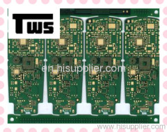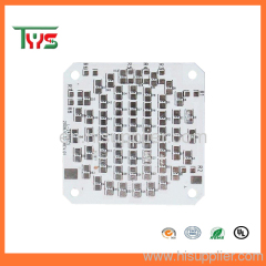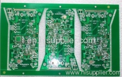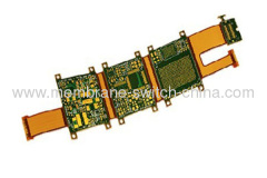
electronic houseware multilayer PCB
0.1~20.0 USD
| Min. Order: | 1 Piece/Pieces |
|---|---|
| Trade Term: | FOB |
| Payment Terms: | L/C, D/P, D/A, T/T, WU |
| Supply Ability: | 10000 |
| Place of Origin: | Guangdong |
Company Profile
| Location: | Shenzhen, Guangdong, China (Mainland) |
|---|---|
| Business Type: | Manufacturer |
| Main Products: | PCB&PCBA |
Product Detail
| Means of Transport: | Ocean, Air, Land |
|---|---|
| Basic material: | FR-4 ,FR-2 ,Taconic ,Rogers ,CEM-1,CEM2 ,ceramic , |
| Finish board thickness: | 0.2mm-6.00mm(8mil-126mil) |
| min core: | 0.075mm(3mil) |
| copper thickness: | 0.5-12oz |
| min.hole diameter for CNC driling: | 0.1mm(4mil) |
| min.hole diameter for punching: | 0.9mm(35mil) |
| biggest panel size: | 610mm*508mm |
| Production Capacity: | 10000 |
| Packing: | vacuum packing |
| Delivery Date: | 3-15 working day |
Product Description
Welcome to XinDaxing PCB&PCBA
Shenzhen Xindaxing ElectricTechnology Co., Ltd.
(Xing Da Electric Technology CO.,Ltd),whichhas been specializing in PCB/PCBA and Electronic components for manyyears.We can prvide a package ofservice:
- 1. PCB layout, PCB design;
- 2: Make high difficulty PCB(1 to 38 layers)
- 3: Provide all Electronic components;
- 4: PCB assembly;
- 5: Write programs for clients;
- 6:PCBA/finished product Test.
- etc…
1.Specification for PCB&PCBA Manufacture:
Item | Specification |
Numbr of Layer | 1-38Layers |
Material | FR-4,FR2.Taconic,Rogers, CEM-1CEM-3,ceramic , crockery |
Metal-backedLaminate | |
Remarks | High Tg CCL IsAvailabe(Tg>=170ºC) |
Finish BoardThickness | 0.2mm-6.00mm(8mil-126mil) |
Minimun CoreThickness | 0.075mm(3mil) |
Copper Thickness | 1/2 oz min;12 ozmax |
Min.Trace Width & LineSpacing | 0.075mm/0.1mm(3mil/4mil) |
Min.Hole Diameter for CNCDriling | 0.1mm(4mil) |
Min.Hole Diameter forpunching | 0.9mm(35mil) |
Biggest panel size | 610mm*508mm |
Hole Positon | +/-0.075mm(3mil) CNCDriling |
Conductor Width(W) | +/-0.05mm(2mil)or |
+/-20% of originalartwork | |
Hole Diameter(H) | PTHL:+/-0.075mm(3mil) |
Non-PTHL:+/-0.05mm(2mil) | |
Outline Tolerance | +/-0.125mm(5mil) CNCRouting |
+/-0.15mm(6mil) byPunching | |
Warp & Twist | 0.70% |
InsulationResistance | 10Kohm-20Mohm |
Conductivity | <50ohm |
Test Voltage | 10-300V |
Panel Size | 110×100mm(min) |
660×600mm(max) | |
Layer-layermisregistration | 4layers:0.15mm(6mil)max |
6layers:0.25mm(10mil)max | |
Min.spacing between hole edge tocircuity pqttern of an inner layer | 0.25mm(10mil) |
Min.spacing between board oulinetocircuitry pattern of an inner layer | 0.25mm(10mil) |
Board thicknesstolerance | 4layers:+/-0.13mm(5mil) |
6layers:+/-0.15mm(6mil) | |
Impedance Control | +/-10% |
Different Impendance | +-/10% |
2.Quoterequirement
1).Many agile forms of cooperation(OEM ,ODM) arewelcome!
2).The detailed files(Gerber files andspecification);
3).Carbon PCB samples forus;
4).Carbon PCB Test method.
Why us?
Quality
Our UL/RoHsstandards insure quality assemblies from start to finish. Whether it's a simplecustom product or a complex turnkey production run, XingDa will adhere to thehighest quality standards.
Capable
XingDa offersthe latest in assembly capabilities and qualifications insuring that quality isbuilt into every product we produce.
Experience
When it comesto your build you want a partner you can depend on. Our management team has over10years of combined industry knowledge. Our engineering team has over 8 yearsexperience.
Protecting yourinterests
Protectingyour Intellectual Property is job one! Our staff colleague of trainedprofessionals are all working under a strict confidentiality contract and treatyour important documentation as they would their own.
Flexibility
XingDa prideourselves on our ability to custom tailor programs around our customers' needs.We take time to listen to your unique business needs and then set out to surpassthem.