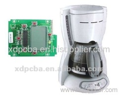
coffe machine PCB Assembly
0.1~20.0 USD
| Min. Order: | 1 Piece/Pieces |
|---|---|
| Trade Term: | FOB |
| Payment Terms: | L/C, D/P, D/A, T/T, WU |
| Supply Ability: | 10000 |
| Place of Origin: | Guangdong |
Company Profile
| Location: | Shenzhen, Guangdong, China (Mainland) |
|---|---|
| Business Type: | Manufacturer |
| Main Products: | PCB&PCBA |
Product Detail
| Model No.: | pcba |
|---|---|
| Means of Transport: | Ocean, Air, Land |
| Basic material: | FR-4 ,FR-2 ,Taconic ,Rogers ,CEM-1,CEM2 ,ceramic , |
| Finish board thickness: | 0.2mm-6.00mm(8mil-126mil) |
| min core: | 0.075mm(3mil) |
| copper thickness: | 0.5-12oz |
| min.hole diameter for CNC driling: | 0.1mm(4mil) |
| min.hole diameter for punching: | 0.9mm(35mil) |
| biggest panel size: | 610mm*508mm |
| Production Capacity: | 10000 |
| Packing: | vacuum packing |
| Delivery Date: | 3-15 working day |
Product Description
Welcome to XingDa Electric Technology Co., Ltd
Xindaxing ElectricTechnology Co., Ltd
Weare professional manufacturer in various PCB and PCBA for many years .We canprovide a reasonable price with high quality products.
XingDa who canprovide a full set of service.such asbelow:
*1. PCB layout, PCB design
* 2: Make high difficulty PCB(1 to 38 layers)
* 3: Provide all Electroniccomponent
*4: PCB assembly
*5: Write programs for clients
* 6:PCBA/finished product Test. etc.
1.specification
Item | Specification | ||
1 | Numberof Layer | 1-38Layers | |
2 | Material | FR-4,FR2.Taconic,Rogers,CEM-1 CEM-3,ceramic , crockery Metal-backed Laminate,Aluminumetc. | |
3 | FinishBoard Thickness | 0.2mm-6.00mm(8mil-126mil) | |
4 | MinimumCore Thickness | 0.075mm(3mil) | |
5 | CopperThickness | 1/2 ozmin;12 oz max | |
6 | Min.Trace Width & Line Spacing | 0.075mm/0.1mm(3mil/4mil) | |
7 | Min.Hole Diameter for CNC Drilling | 0.1mm(4mil) | |
8 | Min.Hole Diameter for punching | 0.9mm(35mil) | |
9 | Biggestpanel size | 610mm*508mm | |
10 | HolePosition | +/-0.075mm(3mil)CNC Drilling | |
11 | ConductorWidth(W) | 0.05mm(2mil)or;+/-20%of original artwork | |
12 | HoleDiameter(H) | PTHL:+/-0.075mm(3mil);Non-PTH L:+/-0.05mm(2mil) | |
13 | OutlineTolerance | 0.125mm(5mil)CNC Routing;+/-0.15mm(6mil) by Punching | |
14 | Warp& Twist | 0.70% | |
15 | InsulationResistance | 10Kohm-20Mohm | |
16 | Conductivity | <50ohm | |
17 | TestVoltage | 10-300V | |
18 | PanelSize | 110×100mm(min);660×600mm(max) | |
19 | Layer-layermisregistration | 4layers:0.15mm(6mil)max;6 layers:0.25mm(10mil)max | |
20 | Min.spacing between hole edge to circuity pattern of an inner layer | 0.25mm(10mil) | |
21 | Min.spacing between board outline to circuitry pattern of an innerlayer | 0.25mm(10mil) | |
22 | Boardthickness tolerance | 4layers:+/-0.13mm(5mil);6 layers:+/-0.15mm(6mil) |
2.Details forPCB Assembly
Technical
1).Professional surface mounting and throughhole soldering technology;
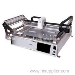
2).Various sizes,like 1206,0805,0603 componentsSMT technology;
3).ICT(In Circuit Test),FCT(Functional CircuitTest) technology;
4).Nitrogen gas reflow soldering technologyfor SMT;
5).High standard SMT&Solder Assemblyline;
6).High density interconnected board placementtechnology capacity.
Quote requirement
1).The detailed files(Gerberfiles,specification andBOM);
2).Clear pictures of PCBA or samples forus;
3).PCBA Test method.