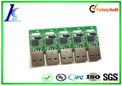
E-testing circuit board.USB charge board with assembly.single-sided PCB for usb connector
0.01~1.2 USD
| Min. Order: | 1 Piece/Pieces |
|---|---|
| Trade Term: | FOB |
| Payment Terms: | Paypal, T/T, WU |
| Supply Ability: | 30000 square meters/month |
| Place of Origin: | Guangdong |
Company Profile
| Location: | Shenzhen, Guangdong, China (Mainland) |
|---|---|
| Business Type: | Manufacturer, Trading Company |
| Main Products: | PCB.PCBA |
Product Detail
| Model No.: | Single-sided PCB-9 |
|---|---|
| Means of Transport: | Ocean, Air, Land |
| Brand Name: | K-better |
| Base Material: | FR4.CEM-1.CEM-3 |
| Copper Thickness: | 0.5-3.0oz |
| Board Thickness: | 0.2-3.0mm |
| Min. Hole Diameter: | 0.25mm |
| Min. Line Width: | 0.15mm |
| Min. Line Spacing: | 0.15mm |
| Surface Finishing: | immersion gold.HASL.HAL lead free.OSP.gold plating |
| certification: | ISO9000.CE,UL,RoHS |
| other service: | pcb/pcba copy.board testing.parts purchase |
| soldermask color: | red.green.black.white.blue.yellow.etc |
| Production Capacity: | 30000 square meters/month |
| Packing: | vacuum packing |
| Delivery Date: | 3-7 days |
Product Description
Warm welcome you desire or inquiries negotiations.
Contribute efforts to you with all sincerity is our commitment.
We are in hopes of your cooperation!
Our Service:
1. Turnkey Service:
Procurement agent component and related electronic products according to your BOM--component's list. Helping you the product with best price and best quality from biggest electrical market in China.
2. SMT, DIP processing
Giving us your sample, design or your idea file, we can hand in you want.
3. Testing&Assembly
Inform us your testing way, we also help you do the testing service, giving you 99% work well perfect product
Our Advantages:
*Our company was established in 1996, which is engaged in printing circuit board production. It has long history.
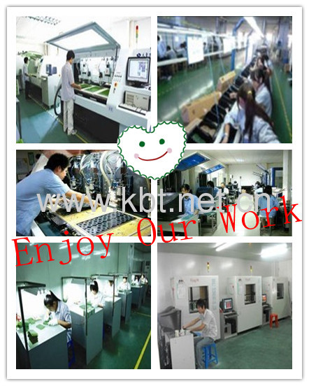
*We have our own factory and equipped with advanced circuit board production line. the digital control drilling machine, optical painting equipment, exposing machine, developing machine and so on.
It can produce a high-quality PCB production.
*Enjoying high reputation in this line.
*Effective management to make every member can do their best for the customer.
*There's no limit in Quantity.
Key Specifications/Special Features:
*Layers: 1 to 16
*Materials: FR-4, CEM-1, aluminum,
*Finish board thickness: 0.2 to 3.2mm
*External copper thickness: 35 to 210um
*Internal copper thickness: 17 to 140um
*Copper plating hole: 18 to 40um
*Trace width and line spacing: 0.075/0.1mm (3/4 mils)
*CNC hole diameter: 0.20mm (minimum)
*Punching hole diameter: 0.9mm (35 mils) (minimum)
*Panel size: 610 x 508mm (maximum)
*Hole position tolerance: 0.075mm
*Hole dimension tolerance: 0.075 (PTH) and 0.05mm (NPTH)
*Outline tolerance: 0.125 (CNS) and 0.15mm (punching)
*Warp and twist: 0.70%
*Solder mask bridge: 0.0635mm (minimum)
*Distance between lines to board bridge: 0.25 (minimum) (outline) and 0.40mm (v-cut)
*Impedance control tolerance: ±10%
*Test voltage: 10 to 300V
*Solder mask types: green, yellow, red, white, blue, matte green, matte black and more
*Surface finished: HASL, immersion gold, immersion silver, gold-plated, gold finger and OSP
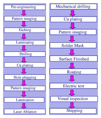
Production Process:
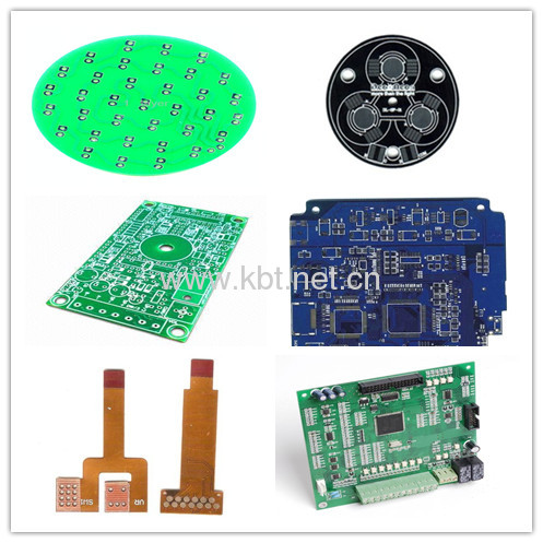
Product Show:
Quick Leadtime:
Lead time for sample | 2-3 days for single-sided board |
4-5 days for double-sided board | |
6-7 days for multilayer board | |
24-48 hours for urgent | |
Lead time for Opening Mould | 3-5 days for normal mould |
5-7 days for hard mould | |
Lead time for Mass production | 5-7 days for single/double sided board |
7-10 days for multilayer board |
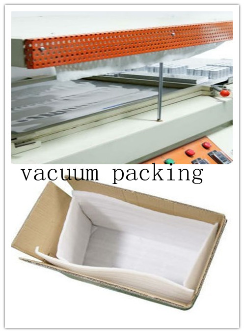
Packing Terms:
(1)Inner packing: all the goods will be packed by vacuum
(2)Outer packing: standard carton
Welcome to visit our Factory:
IF you have any interest
Please contact us at any time..

Welcome to visit our Factory:

IF you have any interest
Please contact us at any time..

