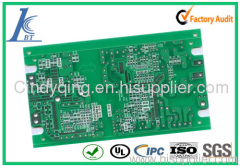
Double-sided PCB with lead free surface treatment, china PCB supplier.
0.1~20.0 USD
| Min. Order: | 1 Piece/Pieces |
|---|---|
| Trade Term: | FOB |
| Payment Terms: | T/T, paypal, WU |
| Supply Ability: | 30000 square meter/month |
| Place of Origin: | Guangdong |
Company Profile
| Location: | Shenzhen, Guangdong, China (Mainland) |
|---|---|
| Business Type: | Manufacturer, Trading Company |
| Main Products: | PCB.PCBA |
Product Detail
| Model No.: | double-sided-2 |
|---|---|
| Means of Transport: | Ocean, Air |
| Brand Name: | K-better |
| Base Material: | FR4.CEM-1.CEM-3 |
| Copper Thickness: | 0.5-3.0oz |
| Board Thickness: | 0.2-3.0mm |
| Min. Hole Size: | 0.25mm |
| Min. Line Width: | 0.15mm |
| Min. Line Spacing: | 0.15mm |
| Surface Finishing: | immersion gold.OSP.HAL.lead free.gold plating |
| certification: | ISO9000.UL |
| Soldermask color: | black.red.green.yellow.blue.etc |
| other service: | PCB&PCBA copy.board testing.parts purchase. |
| Production Capacity: | 30000 square meter/month |
| Packing: | vacuum packing |
| Delivery Date: | 3-7 days |
Product Description
High Quality+Good Service=Confidence
3.The Technical Information of the Product
4. The Product Show

5. What We Need:
6.What can the customer get:
If you have any intertst in our product.
Dear Customers,Welcome to our website.We promise you that we will do our best to provide you high quality product and good service.
Following,Please allow me to introduce our company to you.
1. Brief introduction of Our Company

We are Shenzhen K-better Circuit Electircal Co,.Ltd. Our company was established in 1996.which engaged in Printed Circuit Board Production

We are Shenzhen K-better Circuit Electircal Co,.Ltd. Our company was established in 1996.which engaged in Printed Circuit Board Production
2. The Services of Our Company
We provide following service to all of our customers:
1. PCB production service. Available on FR-4,TG150-180,Aluminum, FPC
2. PCB copy service
3. PCB assembly service. Available on SMT, BGA, DIP.
4. And Box build assemble. Available on Final Functional testing and final package
5. Electronic Component purchasing service
1. PCB production service. Available on FR-4,TG150-180,Aluminum, FPC
2. PCB copy service
3. PCB assembly service. Available on SMT, BGA, DIP.
4. And Box build assemble. Available on Final Functional testing and final package
5. Electronic Component purchasing service
3.The Technical Information of the Product
ITEMS | CAPACITY |
Base material | FR4 |
Copper thickness | 0.5-2.0oz |
Board thickness | 0.2-3.0mm |
Min. Hole size | 0.25mm |
Min. Line width | 0.2mm |
Min. Line spacing | 0.2mm |
Surface finishing | immersion gold.OSP.HASL(Spray tin) |
Sold mask | Red.blue.yellow.black.white.etc. |
Test | E-Testing |
Certification | ISO9000,CE,ROHS |
Lead time | For sample:1-7 days |
For opening mould:3-7 days | |
For mass production:5-10 days | |
Packing | Inner packing: vacuum packing |
Outside packing: Standard carton packing |
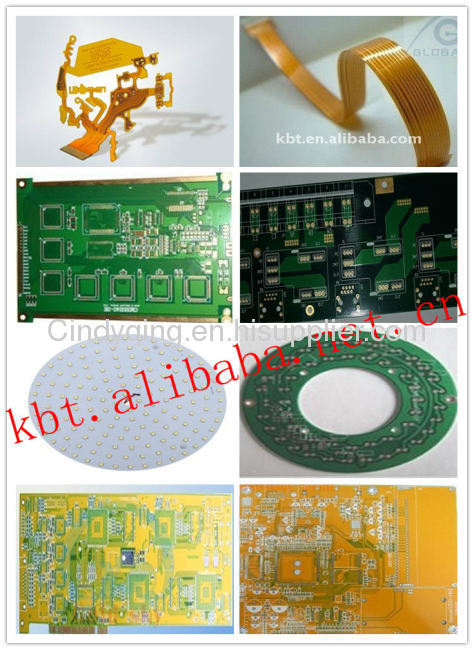
4. The Product Show

5. What We Need:
We need PCB drawing in Gerber, Protel or other softwares.
If the Customer can not provide original PCB drawing, we need samples for cloning.
6.What can the customer get:
Competitive Price, Prompt Delivery, Standard Qualtity, Best Service.
If you have any intertst in our product.
Please contact us at any time.
We are very glad to service for You!

