
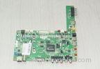
1 - 16 Layer 0.2 - 3.2mm Thickness Routing, Punching Electronic PCB Assembly For MP4, Led
| Place of Origin: | Zhejiang |
|---|
Company Profile
| Location: | Shenzhen, Guangdong, China (Mainland) |
|---|---|
| Business Type: | Manufacturer |
| Main Products: | Single Sided PCB |
Product Detail
| Model No.: | CE, ROHS, UL |
|---|
Product Description
1 - 16 Layer 0.2 - 3.2mm Thickness Routing, Punching Electronic PCB Assembly For MP4, Led
Description:
|
Layer |
1-16 |
|
Material |
FR4 |
|
Thickness |
0.2-3.2mm |
|
Surface finishing |
HAL/ENIG |
|
Copper |
0.5-3oz |
|
Test |
Electrical Test |
A PCB populated with electronic components is called a printed circuit assembly (PCA), printed circuit board assembly or PCB Assembly (PCBA).
After the printed circuit board (PCB) is completed, electronic components must be attached to form a functional printed circuit assembly, or PCA (sometimes called a "printed circuit board assembly" PCBA). In through-hole construction, component leads are inserted in holes. In surface-mount construction, the components are placed on pads or lands on the outer surfaces of the PCB. In both kinds of construction, component leads are electrically and mechanically fixed to the board with a molten metal solder.
Specifications:
|
Product Technical Parameter |
|||
|
Basic technology |
Parameter |
||
|
Single/Double sided |
Multilayer |
||
|
Number of Layers |
1-2 |
4~16 |
|
|
Copper Thickness |
0.25~3.0OZ |
0.5~3.0OZ |
|
|
Base Board Thickness |
0.2~3.2mm |
0.6~3.2mm |
|
|
Incombustibility |
94V-0 |
94V-0 |
|
|
Peelable resistance |
12.3N/cm |
12.3N/cm |
|
|
Twist |
≤0.5% |
≤0.5% |
|
|
Insulation resistance |
≥1011Ω |
≥1011Ω |
|
|
Test voltage |
10-300V |
10-300V |
|
|
Finished board area |
560×970mm |
560×970mm |
|
|
Min. Line Width and Spacing |
|||