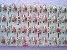
1 - 16 Layer Routing Punching Electrical Test Led Printed Circuit Board With HAL / ENIG
| Place of Origin: | Zhejiang |
|---|
Company Profile
| Location: | Shenzhen, Guangdong, China (Mainland) |
|---|---|
| Business Type: | Manufacturer |
| Main Products: | Single Sided PCB |
Product Detail
| Model No.: | CE, ROHS, UL |
|---|
Product Description
1 - 16 Layer Routing Punching Electrical Test Led Printed Circuit Board With HAL / ENIG
Description:
|
Layer |
1-16 |
|
Material |
FR4 |
|
Thickness |
1.6mm |
|
Surface finishing |
HAL / ENIG |
|
Copper |
1oz |
|
Test |
Electrical Test |
Applications:
LED Printed circuit board are mainly used for different kinds of LED. It’s widely used in various of industries in the world such as market, advertisement, Car, Buildings and so on. We have been pcb/pcba business for ten years and provide different customized pcb to many countries all over the world. Welcome to contact us for further news.
Specifications:
|
Product Technical Parameter |
|||
|
Basic technology |
Parameter |
||
|
Single/Double sided |
Multilayer |
||
|
Number of Layers |
1-2 |
4~16 |
|
|
Copper Thickness |
0.25~3.0OZ |
0.5~3.0OZ |
|
|
Base Board Thickness |
0.2~3.2mm |
0.6~3.2mm |
|
|
Incombustibility |
94V-0 |
94V-0 |
|
|
Peelable resistance |
12.3N/cm |
12.3N/cm |
|
|
Twist |
≤0.5% |
≤0.5% |
|
|
Insulation resistance |
≥1011Ω |
≥1011Ω |
|
|
Test voltage |
10-300V |
10-300V |
|
|
Finished board area |
560×970mm |
560×970mm |
|
|
Min. Line Width and Spacing |
0.1/0.1mm |
0.1/0.1mm |
|

