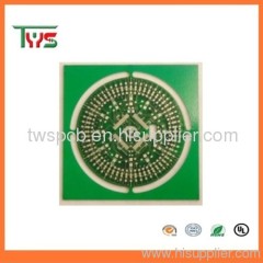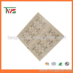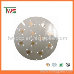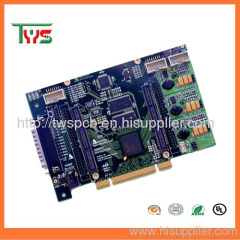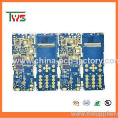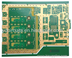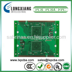
ROHS fr4 4-layer pcb factory
1.0~50.0 USD
| Min. Order: | 1 Piece/Pieces |
|---|---|
| Trade Term: | FOB |
| Payment Terms: | Paypal, T/T, WU |
| Supply Ability: | 20000square meter per month |
| Place of Origin: | Guangdong |
Company Profile
| Location: | Shenzhen, Guangdong, China (Mainland) |
|---|---|
| Business Type: | Manufacturer |
Product Detail
| Model No.: | LX0005 |
|---|---|
| Means of Transport: | Ocean, Air, Land |
| Number of Layers: | 4-Layer |
| Brand Name: | LX |
| Base Material: | FR4 |
| Copper Thickness: | 1OZ |
| Board Thickness: | 1.6mm |
| Min. Hole Size: | 0.3mm |
| Min. Line Width: | 0.2mm |
| Min. Line Spacing: | 0.2mm |
| solder mask color: | LPI Green mask |
| Production Capacity: | 20000square meter per month |
| Packing: | Inner:vacuum package; Outer:carton |
| Delivery Date: | 5~7days |
Product Description
Our pcb capability
1) Layer: 1-28layers
2) Board finished thickness: 0.21mm-7.0mm
3) Material: FR-4, CEM-1,CEM-3, High TG, FR4 Halogen Free,Rogers,Aluminum
4) Max. finished board size: 23 × 25 ( 580mm×900mm )
5) Min. drilled hole size: 3mil (0.075mm)
6) Min. Line width: 3mil (0.075mm)
Min.Line spacing:3mil (0.075mm)
7) Surface finish/treatment : HASL / HASL lead free,HAL, Chemical tin,Chemical Gold, Immersion Silver/Gold,OSP,Gold plating
8) Copper thickness: 0.5-7.0 OZ
9) Solder mask color: green/yellow/black/white/red/blue
10) Copper thickness in hole: >25.0 um (>1mil)
11)Inner packing: Vacuum packing / Plastic bag
Outer packing: Standard carton packing
12) Shape tolerance: ±0.13
Hole tolerance: PTH: ±0.076 NPTH: ±0.05
13) Certificate: UL, ISO 9001, ISO 14001,
14) Special requirements: Buried and blind vias+controlled impedance +BGA
15) Profiling: Punching, Routing, V-CUT, Beveling
16) Provides OEM services to all sorts of printed circuit board assembly as well as electronic encased products.
The quick-turn service
24 hours for 2-Layer sample
48 hours for 4-Layer sample
72 hours for 6-Layer sample


