
Fiber Optic Devices Telecommunication PCBA | Electronic Manufacturing Services
| Min. Order: | 1 Piece/Pieces |
|---|---|
| Trade Term: | EXW |
| Payment Terms: | L/C, T/T |
| Supply Ability: | 200000pcs per month |
| Place of Origin: | Guangdong |
Company Profile
| Location: | Shenzhen, Guangdong, China (Mainland) |
|---|---|
| Business Type: | Manufacturer, Service |
Product Detail
| Model No.: | pcba-85 |
|---|---|
| Means of Transport: | Ocean, Air |
| 2 layers: | FR4 |
| Production Capacity: | 200000pcs per month |
| Packing: | bubble bag and regular carton |
| Delivery Date: | 2-3 weeks |
Product Description
Supplier: Shenzhen Grande Electronics
Layers: 4
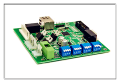
Application: Fiber Optic Devices Telecommunication PCBA | Electronic Manufacturing Services
PCB:FR-4/1.6mm,1oz finished copper
Surface Treatment: ENIG
PCBA Lead time: 3-4 weeks
Packing: Anti-static bag and compartmental packing
Standard Warp: <0.75%
[Description]
1, Turnkey solution for Fiber Optic Devices Telecommunication PCBA | Electronic Manufacturing Services.
2, PCB Assembly, PCB fabrication / PCB layout, PCB re-layout.
3, Electronic Contract Manufacturing.
4, SMT&DIP&PTH&BGA.
5, Components Sourcing.
6, Quick PCBA prototype.
7, X-ray test, the Internal Circuit Test (ICT) , Functional Test (FCT)
8, Sample and small batch order are accepted.
PCBA Service
Customer offers: Gerber file, PCB Specification, BOM and Assembly Drawing.
Full-turnkey PCBA: 1-30Layers PCB, Components Sourcing, SMT, PCBA testing, PCBA Aging test, PCBA Packing and PCBA Shipping.
PCBA Quality Assurance
1, Certifications: UL, SGS, TUV, BV, ROHS, ISO9001: 2008, TS16949: 2008
2, 7 lines dust-proof SMT lines and DIP lines.
3, All line works wear anti-static and dust-proof clothing.
4, All operators should pass strictly training before they start work.
5, SMT Equipment:solder paste printer in Jidakang,, Mounter in Panasonic, Re-flow, Wave Soldering, Semi-auto DIP
6, PCBA Test Equipment: ORT, Constant temperature and humidity chamber,3D CMM,X-Ray.
7, PCBA Test:ICT, Functional Circuit Test and X-ray test.
8, Package Processed:
0402, 0603, 0805, 1206, 1608, 2125, 3216
Micro QFP 0.2mm
Flip-chip, BGA, Connectors
BGA Ball Pitch=0.2mm
9, Each workstation in accordance with the SOP
10, Materials:FR-4, FPC, Aluminum,High TG,Halogen-Free, HF, CEM-1, CEM-3, FR-1, 94-V0 and so on.
11, Material Brand:KB, SHENGYI, NANYA and so on.
PCBA Lead Time
PCBA prototype: 7-10 working days after contract signed and EQ confirmed.
Mass production: partial delivery according to the customer's requirement.
Other information for PCBA
1, The mass production will be arranged after PCBA prototype confirmed.
2, Use Teflon adhesive tape to protect Mount Holes and GND Holes.
3, EPE is used to avoid impact and crash.
PCBA Standard Packing
Anti-static bag and compartmental packing